Practice Making a PCB
Practice Making a PCB
This page contains a practice assignment for making a schematic and a pcb. Refer to the PCB_Artist tutorial for information on how to finish it.
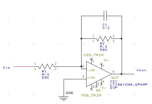
We are going to make a leaky integrator schematic and pcb. You can read about leaky integrators here in the integrator section. This circuit will consist of 2 resistors, 1 capacitor and an op-amp (such as LT1001CN8).
Make the Schematic
We are going to make the following schematic.
You already have the resistor and capacitor components, but the op-amp component does not exist yet.
Search for a datasheet of the LT1001CN8 precision operational amplifier. (You can search on google, digikey...etc).
To create the schematic symbol, you can either draw your own schematic for the 8pin op-amp as shown above OR you can find the existing schematic symbol under one of the existing libraries (hint op-amps are integrated circuits(IC)). If you make your own, make sure you have 8 pins.
You will have to make the pcb footprint for this op-amp using the tools from the tutorial.
Create a component and name the pins as shown in this schematic (ie IN-,IN+,etc)
You will need to add extra text for Vin and Vout.
Make the PCB
Now we will make the PCB of this circuit.
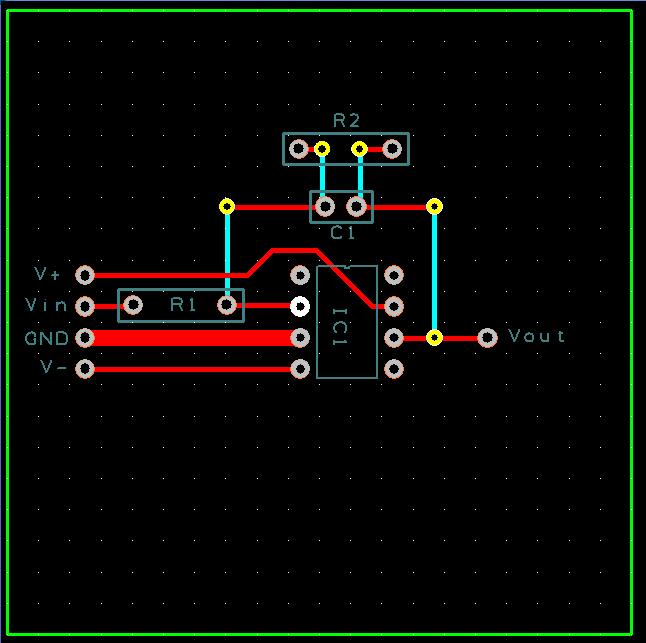
The finished board should look like this:
Use 'Translate to PCB' as in the tutorial to convert your schematic into a pcb.
In the PCB configuration
- Create a 2x2 in pre-defined board
- Basic 2 Layer Standard
- Default Layers and Board Parameters
- Special Requirement - Student
- Name your board with a 1 week turn around time and quantity of 1.
On your board, make sure you:
- Add 5 extra pins for Vin, Vout, V+, V- and GND
- Add silkscreen text for these 5 extra pins
- Change the trace size between GND and the op-amp to have a width of 0.05
- 5 vias as shown above
- 1 mitered track as shown above

