Driving a high current DC Motor using an H-bridge
Overview
An H-bridge is a common circuit used to control the speed and direction of a brushed DC motor. The convenience of an H-bridge is that a low current PWM signal can be used to control a high current motor (or other device). Full H-bridge circuits capable of a few Amps can be purchased in convenient IC packages (see PWM and H-bridge chips). The H-bridge described in this write-up is capable of currents up to about 40A at 24V.
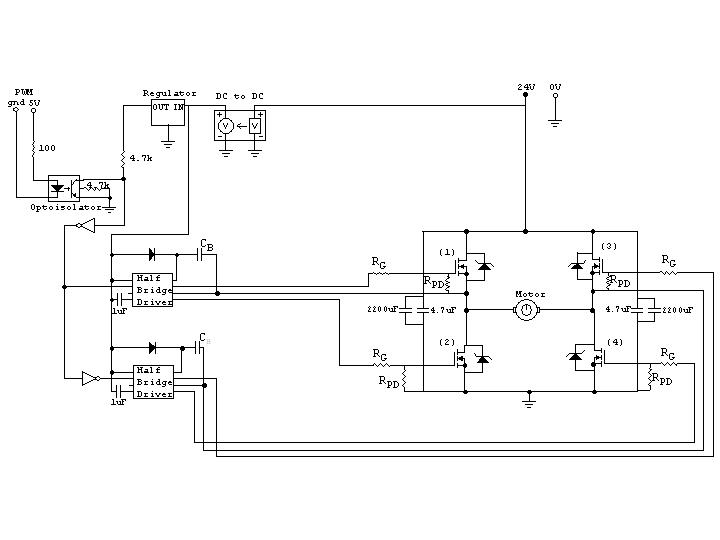
In the circuit diagram we see that the 4 mosfets surrounding the motor form an “H” shape. The mosfets are used as switches and are activated in diagonal pairs. To apply a forward voltage across the motor, mosfets 1=4=on and 2=3=off, causing the motor to spin in the forward direction (PWM=100% duty cycle). To make the motor spin in reverse, 1=4=off and 2=3=on (PWM=0% duty cycle).
To keep the motor stationary, forward voltage is applied half of the time and reverse voltage is applied half of the time (PWM=50% duty). If the voltage reversals are at a high enough frequency, the cycling is unnoticeable. Generally 20kHz is a good choice for PWM frequency because it is well beyond of the dynamic range of motors and just beyond the range of human hearing. For more information on PWM, see Driving a DC Motor using PWM and Pulse Width Modulation.
While the concept of a high current H-bridge is fairly simple, many practical considerations complicate implementation.
| Component | Value/Part# |
|---|---|
| MOSFETS | STP80NF55-08 (80A 55V) |
| Half Bridge Driver | IR2109 |
| DC to DC converter | VBSD1-S24-S12-SIP (24V to 12V) |
| Regulator | 78L05 (5V) |
| Inverters | SN74HC14N |
| Optoisolator | 4N270545K |
| C_B | 0.1 uF |
| R_G | 4.7 Failed to parse (MathML with SVG or PNG fallback (recommended for modern browsers and accessibility tools): Invalid response ("Math extension cannot connect to Restbase.") from server "https://wikimedia.org/api/rest_v1/":): {\displaystyle \Omega} |
| R_PD | 2.2 kFailed to parse (MathML with SVG or PNG fallback (recommended for modern browsers and accessibility tools): Invalid response ("Math extension cannot connect to Restbase.") from server "https://wikimedia.org/api/rest_v1/":): {\displaystyle \Omega} |
The example H-bridge above works with a 24V supply and all of the specified components. If you need to change a component, it is very likely that the other components will need to be re-sized. Some rules-of-thumb for each component are provided below.
Implementation Considerations
Electrical Noise
The motor can create significant electrical noise because it draws a great deal of current causing dips and spikes in the power supply, and more significantly, when the mosfets abruptly cut off the current, the motor's inductance creates voltage spikes (as predicted by: V = L*di/dt).
To prevent the noise from having a deleterious effect on the mosfets, there is significant capacitance in close proximity to the mosfets. The diodes (that often come integrated into the mosfets) also play an important role here. If the motor is being driven forward (1=4=on) and then all mosfets are turned off, there will be a voltage spike due to the inductance of the motor. This spike can dissipate by drawing current through the diodes in mosfets 1 and 3, effectively sending the current into the capacitors and battery.
It is also possible to reduce the inductive voltage spikes by increasing the time it takes to transition between states. This can be accomplished by increasing the Gate Resistance (covered later).
Shoot Through
It is important to ensure that the two mosfets on the same half-bridge are never on at the same time. This condition called “shoot through”, shorts the power supply and will likely damage the mosfets. The IR2109 half bridge driver chip contains logic to prevent this condition from occurring. It outputs the PWM signal to the high mosfet gate while sending an inverted version of the signal to the low mosfet gate. To be certain that shoot through does not occur during the transient, it also adds a 540ns dead time where both signals are low.
High Mosfet Gate Voltage
To turn an N-channel mosfet to its “on” state, it is necessary to raise its gate voltage (Vgs) 2-10V above the source voltage (note that the pins on a N-channel mosfet are deceivingly named: the low-voltage side of the mosfet is the “source”). In our example this means that when the high mosfet is turned on the voltage at the source pin (the high side of the motor) is 24V so the voltage at the gate must be about 34V. The half-bridge driver chip is able to supply this high voltage by using a bootstrapping circuit.
The bootstrapping method for achieving the high mosfet gate voltages avoids the need for an additional DC to DC power supply, but for the bootstrapping to work, there needs to be time to recharge the bootstrapping capacitor. That means that this H-bridge cannot be run at 0% or 100% duty cycle. At 20kHz, the maximum forward and reverse speeds occur at about 10% and 90% duty cycle.
The gate for a mosfet acts like a capacitor, and once the “gate charge” is reached, the mosfet is in its “on” state. Gate charge can be found on the data sheet and is usually in the units of nanocoulombs (nC). To estimate the half-bridge driver current demand we only need to consider how many times this charge will be applied each second.
Half_Bridge_Driver_Current (A) = Gate_Charge (C) * PWM_freq (Hz)
PCB Current Capability
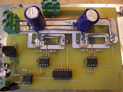
It is possible to get a printed circuit board (PCB) made with very thick traces, but it is often significantly cheaper to stick with copper trace weight of 1oz/ft^2. Based on a Trace Width Calculator the 0.340" tracks on the included PCB file can handle about 20 Amps. To increase its current carrying ability, we soldered 14AWG solid copper wire in parallel with the high-current PCB traces.
The board shown in the picture has been succeeded by this board H bridge PCB file, which has been corrected and improved, but not tested. Use at your own risk.
Energy Dissipation
Significant energy is dissipated by the mosfet whenever the gate is not fully on or fully off. This causes heating problems and reduces efficiency. Energy dissipation can be minimized by making quick transition between the off and on states. It can also be minimized by reducing the PWM frequency. The lower the PWM frequency, the less transitions there are in a given time period, unfortunately it is generally necessary to set the PWM frequency above 18kHz to make it inaudible.
Component Selection
MOSFETS
The example H-bridge uses N-channel mosfets. IGBTs can also be easily used. P-channel mosfets are often used for the high mosfets in an H-bridge, but there is a cost penalty [ref], and it is unnecessary because there are many half-bridge driver chips set up for N-channel mosfet half-bridges.
It is advisable to pick a mosfet that is rated for twice the expected voltage and current [ref]. In the example H-bridge, the battery is 24V and predicted stall current was ~50A, when we used Mosfets rated for 30V we regularly had catastrophic failures. 55V, 80A mosfets were a much more robust solution.
Most power mosfets have an integrated Free Wheeling Diode (FWD), but is worth noting here that without these diodes, the inductive voltage spikes will destroy the mosfets.
Boot Strapping Capacitor (C_B)
The bootstrapping capacitor should be sized large enough such that it can provide enough charge to keep the gate on for the duration of the PWM duty cycle.
Since the example circuit does not have a watchdog functionality, it is also necessary to make sure the bootstrapping capacitor is not too large. If the bootstrapping capacitor is too large and the mosfet is held in the on state for a long period of time, the capacitor will slowly discharge and Vgs will slowly transition from 10V to 0V. Since the micro-controller keeps the motor stationary by maintaining a 50% duty cycle, this condition can easily occur when the micro-controller is reset and a 0% duty cycle (full reverse) is sent to the H-bridge. The most noticeable effect is that powering down the micro-controller will cause the motor to lurch in reverse. Also, keeping Vgs in the half-on state for a long period can damage the mosfet because the large voltage drop between the drain and the source will dissipate significant energy.
In general, increasing the mosfet “gate charge” will necessitate an increase in the Cb value.
Gate Resistors (R_G)
It is generally important to have crisp transitions between the off and on states of the mosfet so that it does not spend significant time in its half-on state dissipating energy. Unfortunately, it can also be detrimental to switch the state too quickly for two reasons: 1. the more quickly the current is cut off, the larger the inductive voltage spikes (V=L*di/dt). 2. mosfet data sheets often specify a maximum “dv/dt” rating that refers to the maximum allowable time derivative of Vgs.
To prevent the mosfet from switching too quickly, a small amount of gate resistance is added (usually 2-50Failed to parse (MathML with SVG or PNG fallback (recommended for modern browsers and accessibility tools): Invalid response ("Math extension cannot connect to Restbase.") from server "https://wikimedia.org/api/rest_v1/":): {\displaystyle \Omega} ) to increase the time it takes to charge the mosfet gate. If a mosfet with larger gate charge is used, it is sometime necessary to reduce the gate resistance in order to achieve similar switching times.
Pull Down Resistors (R_PD)
Some gate drivers require pull down resistors (R_PD). The IR2109 works without them at the intended frequency of operation, but during robustness tests, where frequency was swept from 1Hz to 200kHz and duty cycle from 0% to 100%, we found that the pull down resistors consistently turned off the gates while the IR2109 alone sometimes failed.
Lower valued pull down resistors generally improve gate-turn-off consistency, but necessitate a larger boot strapping capacitor since current is continually leaked to ground.
Power Capacitors
In the example H-bridge we have two 2200uF capacitors to smooth out the power supply voltage and two 4.7uF ceramic capacitors to smooth out the ultra-high frequency noise on the power supply. The power supply and the wiring to the H-bridge have a non-zero impedance. Without large power capacitors near the mosfets, voltages on the gate, drain and source connections cannot be maintained as desired and the mosfets will over heat or experience catastrophic failures.
Optocoupler and Inverters
To prevent the noisy H-bridge circuit from affecting the other circuits in the system, the PWM input to the H-bridge is optically isolated. Since the optocoupler does not produce a square wave with crisp transitions, it is advisable to add a comparator. In our example we needed an inverter chip for the second half-bridge so we used an inverter as a comparator. Even without optical isolation, it is wise to including these two inverters to ensure crisp, unambiguous transitions between states.
Heat Sinking
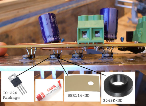
To achieve the amperage rating on a mosfet it is necessary to heat sink it. The heat sink tab on the mosfet is often electrically connected to the drain so it is necessary to electrically isolate the mosfet from the heat sink (often a piece of aluminum). To ensure electrical isolation from the heat sink, a "heat pad" can be purchased to provide a thermally conductive, electrically insulating layer (Ex: part# BER114-ND works for the TO-220 mosfet package). To keep the metal screw from creating an electrical connection, an insulating shoulder washer/bushing (Ex: 3049K-ND) should be used. It is advisable to improve heat transfer using Silicone Heat Transfer Compound (also electrically insulating and thermally conductive). More information on heat sinking is in this article:Driving using a single MOSFET.
Summary of Recommended Improvements
-Add a watchdog circuit to shut down the half-bridge drivers when the PWM signal is missing. There is a "shut down" pin on most half bridge drivers. This would be a generally good idea and allow the bootstrapping capacitor to be set to a large value.
-Instead of bootstrapping to achieve high voltages, use an isolated DC power supply. This would allow the full range of duty cycles from 0-100%.
References
- Valentine, Richard, "Motor Control Electronics Handbook"


