Difference between revisions of "PCB Artist"
(Contact Advanced Circuits:) |
Andrew Long (talk | contribs) |
||
| (91 intermediate revisions by 5 users not shown) | |||
| Line 1: | Line 1: | ||
[[image: |
[[image:CircuitBoard.jpg|400px|right]] |
||
== What is a PCB? == |
|||
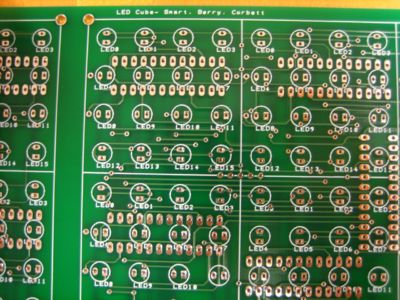
A printed circuit board, or PCB, is an epoxy board clad with copper sheets to make electrical connections along fixed routes. A PCB can have many layers of copper and insulator, depending on the complexity of the design. Layers are connected with vias, plated holes maintaining electrical conductivity. A finished PCB is often covered with solder mask, a solder-phobic layer that helps prevent solder bridges, making the PCB green. A white silk screen can be drawn on top of this, used to label the outlines of components and give other critical information. For more information on PCBs, see the wikipedia page [http://en.wikipedia.org/wiki/Printed_circuit_board Printed Circuit Board]. |
|||
PCBs are created in a variety of ways. A common method is covering the copper you wish to keep and dipping the board in acid, which etches away the copper you do not want. This method can be done by hand. |
|||
A more professional and reliable PCB can be made by designing your circuit in CAD software and ordering the part from a PCB production house. The remainder of this page will describe how to use the proprietary software PCB Artist to design and order a complete PCB. |
|||
== Advanced Circuits and PCB Artist == |
== Advanced Circuits and PCB Artist == |
||
Advanced Circuits [http://www.4pcb.com (www.4pcb.com)] is a company based in Colorado known for their quick turn |
Advanced Circuits [http://www.4pcb.com (www.4pcb.com)] is a company based in Colorado known for their quick turn-around and good prices on low volume printed circuit board (PCB) orders. This is the main supplier for PCBs created by students for clases or research at Northwestern. |
||
Previously, the PCB was created in TraxxMaker or other CAD PCB program, many of which are outdated and difficult to use. Advanced Circuits has created PCB Artist, free software to create schematics and PCBs. This software is designed to order only from Advanced Circuits |
Previously, the PCB was created in TraxxMaker or other CAD PCB program, many of which are outdated and difficult to use, then uploaded to Advanced Circuits. Advanced Circuits has created PCB Artist, free software to create schematics and PCBs. This software is designed to order only from Advanced Circuits. This somewhat simplistic software is very intuitive (once comfortable) and allows for simple changes and editing. Additionally, the component library offered is up to date and contains many specific components. This Wiki page will cover the development and ordering process of a simple PCB board. |
||
<br clear=all> |
|||
===Contact at Advanced Circuits=== |
====Contact at Advanced Circuits==== |
||
Jackie Sartin - Regional Sales Manager |
Jackie Sartin - Regional Sales Manager |
||
| Line 15: | Line 21: | ||
Call: 1-800-979-4PCB (4722) Ext: 1685 |
Call: 1-800-979-4PCB (4722) Ext: 1685 |
||
== Getting Set |
== Getting Set Up == |
||
Have a complete circuit schematic and know exactly what parts (including part numbers) you are using. |
*Have a complete circuit schematic and know exactly what parts (including part numbers) you are using. |
||
[http://www.4pcb.com/index.php?load=content&page_id=46 Download the software] |
|||
Or, type “PCB Artist” into google. |
|||
Click the download button in the middle of the screen. |
|||
[http://www.4pcb.com/index.php?load=content&page_id= |
*[http://www.4pcb.com/index.php?load=content&page_id=46 Download the software] Or, type “PCB Artist” into google. Then click the download button in the middle of the screen. |
||
*Review the material on this page: [http://www.4pcb.com/index.php?load=content&page_id=306 Help Guides and User Reference documents] |
|||
Browse through the [http://www.4pcb.com/downloads/pcbartist/PCBArtistTutorial.pdf Advanced Circuits tutorial pdf] to get familiar with the program interface and design process. In general, you will: |
|||
<br clear=all> |
|||
*Create a schematic (.sch) that represents the circuit you want to create. This schematic is just like any other schematic you would draw by hand, but it will be used to automate the process of laying out your physical PCB and is very helpful in debugging. |
|||
== Advantages / Disadvantages of Robotic Snake Motion == |
|||
*Create a PCB design (.pcb) that represents your physical PCB, based on your schematic. In this CAD process, the program will automatically grab the components you need and place them outside of the board. You then place each component and connect the pins based on how they are connected in the schematic. The program helps you by highlighting the nets (all the pins that need to be connected) in different colors. You choose how to connect each pin, the width of the copper trace, the layer the copper should be on (top or bottom for a 2 sided board), and the size of the vias. You can have PCB Artist automatically place your components and connect them, but the result may not be pretty or successful. |
|||
===Advantages=== |
|||
*Check for errors. Use the Design Rule Check tool to make sure the board is machinable and the pins are connected as they are in your schematic. Carefully scan your board to make sure vias don't accidentally touch traces. Put some silk screen labels next to pins and components, and put your name and the version of your board somewhere for later reference. |
|||
Many robots are limited by the use of motorized wheels. However, there are many advantages for building a robot that mimics the motion of a snake. Several advantages for movement of a snake robot are listed below: |
|||
*Order your board! Use the student deal ($33 for one board), but note it generally takes a week to make and a few days to ship (another $15). So order early and design carefully. |
|||
*Move across uneven terrain, since it is not dependent on wheels |
|||
*Possibly swim if water-proofed |
|||
*Move across soft ground such as sand, since it can distribute its weight across a wider area |
|||
Some general tips: |
|||
Also, from a systems standpoint, the snake robot can be very modular with many redundant segments. As a result, it is very easy to replace broken segments as well as shorten or lengthen the robot. |
|||
*Don't try to make a 2" x 2" board if your space constraints allow for a larger board. It is not worth the effort and possible mistakes trying to squeeze everything into a tiny area if you don't have to. |
|||
===Disadvantages=== |
|||
*Connect your power and ground traces first, they are usually the most complicated. |
|||
Although there are many advantages for building a snake like robot, there are several disadvantages which are listed below: |
|||
*Try to keep an organized board. Keep components with many connections close together. |
|||
*Low power and movement efficiency |
|||
*High cost of actuators (servos or motors) |
|||
*Difficult to control high number of degrees of freedom |
|||
*Use a convention like top layer traces go left-right and bottom layer traces go up-down, this will make routing much easier. |
|||
(Ma, 206) |
|||
*Give yourself some prototyping area and add extra vias to traces. Thus will allow you some wiggle room when your board arrives and has errors (every board will have some errors!). Traces can be cut with a razor blade fairly easily if the board is not too tight, and can be remade with wires if you remember to leave some extra vias around to solder to. |
|||
== Robot Snake Motion == |
|||
[[image:Serpentine_curves.jpg|thumb|300pix|right|Serpentine Curves]] |
|||
==Download and Installation Instructions== |
|||
Real snake motion does not follow specified equations. However, research has proven that the serpentine motion of a snake can be modeled with the following equations (Saito etal, 72-73): |
|||
Download and install PCB Artist from Advanced Circuits at [http://www.4pcb.com/index.php?load=content&page_id=46 the Advanced Artist website.] The latest version as of 1/7/2010 is 1.3.2. It is PC only and works best in Windows XP. |
|||
<math>x(s)= \int_{0}^{s} \cos (\zeta_\sigma) d\sigma</math> |
|||
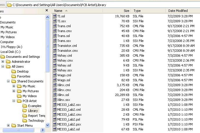
To install a library, download [[Media:ME333_Lab22.zip | the example .zip file here]]. Extract the files and place them in the PCB Artist Library folder. On Windows XP the default location is: C:\Documents and Settings\All Users\Documents\PCB Artist\Library, and on Windows Vista or Windows 7 the default location is C:\Users\Public\Documents\PCB Artist\Library. |
|||
<math>y(s)= \int_{0}^{s} \sin (\zeta_\sigma) d\sigma </math> |
|||
[[Image:library.jpg]] |
|||
<math>\zeta_\sigma= a \cos (b\sigma) +c\sigma </math> |
|||
==Create a Schematic== |
|||
where the parameters ''a'', ''b'', and ''c'' determine the shape of the serpentine motion. The graph shows how the parameters influence the serpentine curve. Basically, ''a'' changes the appearance of the curve, ''b'' changes the number of phases, and ''c'' changes the direction. |
|||
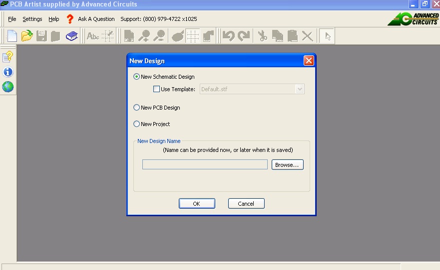
Open a new schematic. |
|||
[[Image:new_schematic.jpg]] |
|||
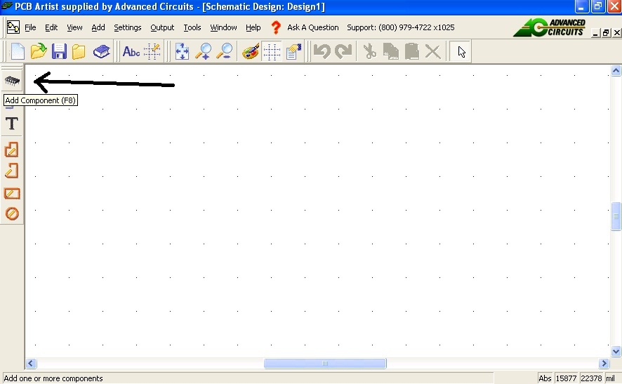
Select Add a Component. |
|||
The serpentine curve can be modeled with a snake like robot by changing the relative angles between the snake robot segments using the following formula with the number of segments (n): |
|||
[[Image:select_component.jpg]] |
|||
Choose the library your component is in (the ME333 library). |
|||
<math>\phi_i = \alpha sin(\omega t +(i-1)\beta ) + \gamma, \left ( i=1, ..., n-1 \right )</math> |
|||
[[Image:select_schematic_library.jpg]] |
|||
where α , β , and γ are parameters used to characterize the serpentine curve and are dependent on ''a'', ''b'', and ''c'' as shown below: |
|||
Place the component R-3. Components should be arranged so that the schematic can be read and understood easily, they do not need to be laid out as they would on the PCB, we will do that later. To drag components around in the schematic, click the arrow button in the toolbar at the top to get the arrow cursor. |
|||
[[Image:place_schematic_component.jpg]] |
|||
<math>\alpha = a \left | \sin \left ( \frac{\beta}{2} \right ) \right | </math> |
|||
Add the LED from the ME333 library and connect the components using the Add Schematic Connection tool (the icon on the left that looks like a pencil drawing a line). Such connections will make it easier to create the PCB. They indicate which pins need to be connected on the PCB, but they do not represent the actual paths the traces will take. We will design those later. |
|||
<math>\beta = \frac{b}{n} </math> |
|||
[[Image:connect_schematic_components.jpg]] |
|||
<math>\gamma = -\frac{c}{n} </math> |
|||
Add a voltage source and ground from the Schema library and connect them to the schematic. |
|||
[[Image:complete_schematic.jpg]] |
|||
The equations above for φ<sub>i</sub>,α,β, and γ were used in this snake like robot as shown in the [[Robot Snake#PIC Code|code section]]. |
|||
Save the file (.sch). Now we can design a PCB for this circuit. |
|||
<br clear=all> |
|||
==Create PCB from Schematic== |
|||
== Mechanical Design == |
|||
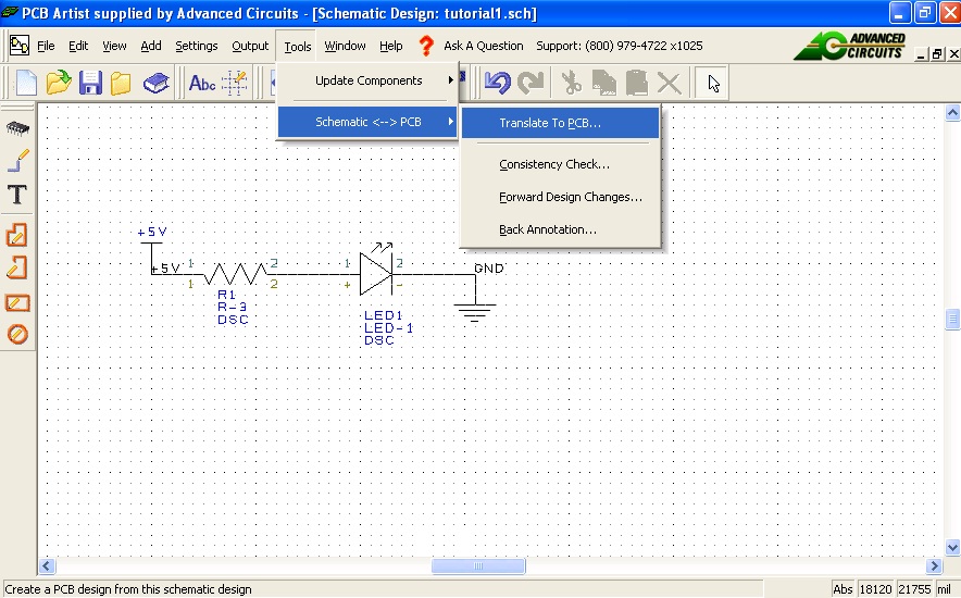
Open your schematic and go to Tools, Schematic <--> PCB, Translate to PCB. |
|||
[[image:FullSnake.jpg|thumb|right|The Snake]] |
|||
The robotic snake consists of a head segment and several body segments. The head segment houses the onboard microcontroller and xBee radio. The body segments house the servo motors and the batteries required to power each motor. As the snake is designed to be modular, there is no limit to the number of body segments. More segments will allow it to move more smoothly, while fewer segments will be easier to control. For this design, seven body segments were used due to material limitations. |
|||
[[Image:translate_to_pcb.jpg]] |
|||
Mechanically, the snake is designed to move in a serpentine motion, imitating the motion of a real snake. As discussed above, real snakes move with anisotropic coefficients of friction. It is difficult to locate materials with this property, but passive wheels satisfy the friction requirements. The friction will be lower in the direction of rolling, thus providing the required difference in friction. The only problem with this approach is that the wheel may slide in the normal direction if the weight applied to the wheel is not sufficient. |
|||
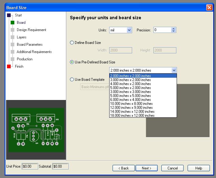
Go through the New PCB Wizard, selecting your board size or defining a custom size. This can always be changed later if you need a larger or smaller board. |
|||
===Parts List=== |
|||
[[Image:board_size.jpg]] |
|||
*Motors: Futaba S3004 standard ball bearing RC servo motor, Tower Hobbies LXZV41 $12.99 |
|||
*Wheels: McMasterCarr Acetal Pulley for Fibrous Rope for 1/4" Rope Diameter, 3/4" OD McMasterCarr 8901T11 $1.66 |
|||
*O-Rings (Tires): McMasterCarr Silicone O-Ring AS568A Dash Number 207, Packs of 50 McMasterCarr 9396K209 $7.60/50 |
|||
*PVC Pipe: McMasterCarr Sewer & Drain Thin-Wall PVC Pipe Non-Perforated, 3" X 4-1/2' L, Light Green McMasterCarr 2426K24 $7.06 |
|||
*1/8th inch plastic for chassis: (Shop Stock) or McMasterCarr Polycarbonate Sheet 1/8" Thick, 12" X 12", Clear, McMasterCarr, 8574K26 $6.32 |
|||
*Dowel Pins: 1" long, 1/4" diameter |
|||
*Sheet Metal: For the connecting segments |
|||
*Fasteners: Screws for the servos and chassis, washers for the standoffs |
|||
*Standoffs: Used 1" and 1/2" to achieve a level snake |
|||
*Velcro: To attach battery packs and housing to the chasis |
|||
*Ball caster: For the head |
|||
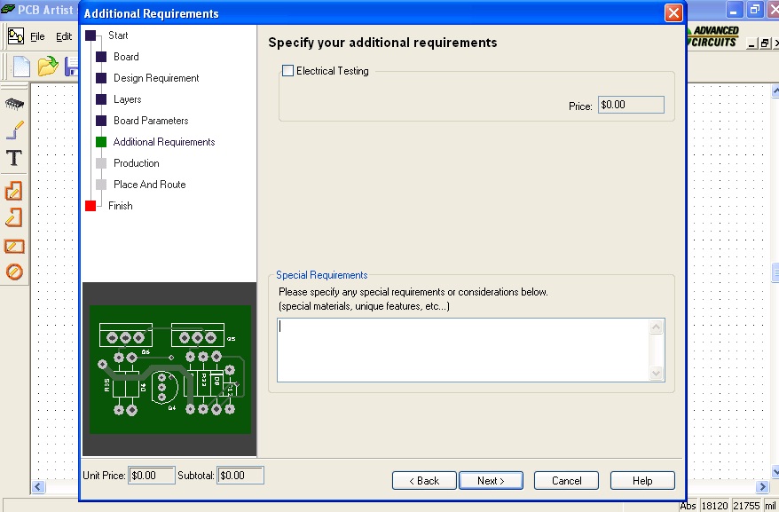
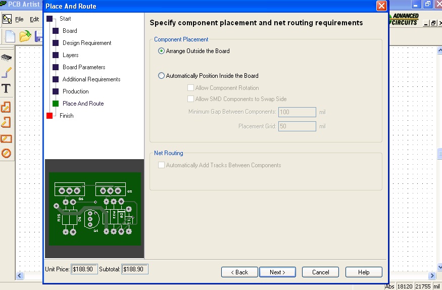
Use a 2 layer board with the default properties. At this screen, |
|||
[[Image:special_reqs.jpg]] |
|||
=== The Body Segments === |
|||
[[image:Chasis.jpg|thumb|right|A Single Chasis Without a Servo]] |
|||
do not enter anything, but later we will add a comment to allow us to buy a Student discount board for $33 plus shipping. |
|||
Each of the body segments are identical and includes a chassis, a servo, a connector, standoffs and two passive wheels as can be seen in the picture. |
|||
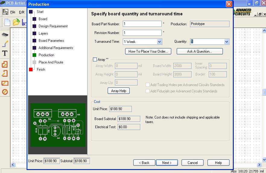
Enter a board number and revision number. Use a 1 week turn around with 1 unit. Ignore the cost, that will change to $33 later. |
|||
[http://www.youtube.com/watch?v=wBcJkNHEaAs Video of 3 body segments moving] |
|||
[[Image:pcb_production.jpg]] |
|||
==== Chassis ==== |
|||
Have the program place the components outside of your board so you can arrange them where you want them. |
|||
The base of the chassis is made from a thin (approx. 1/8th inch) piece of polycarbonate. The chassis must be wide enough to hold a servo motor with a AAA battery pack on each side and long enough for the servo and a standoff (the connection for the previous segment). The polycarbonate was cut into a rectangle to meet the specifications for our servo motor. Five holes were then drilled in the rectangle, four to mount the servo and one for the standoff. The holes are drilled to allow the servo to be located in the center of the chassis. |
|||
[[Image:place_components.jpg]] |
|||
==== Connector ==== |
|||
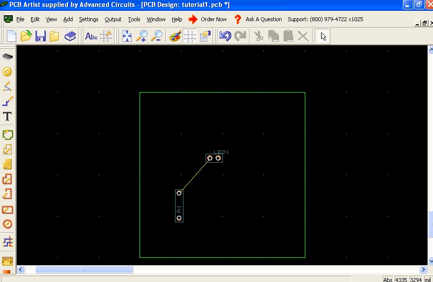
Translate the components to the inside of the green box which represents the outline of your board. Rotate a component by right clicking on the part and choosing rotate. All of the components must be moved inside of the green box to finish the board. These will be their locations on the board. |
|||
A connector was machined to attach to the servo horn of one body segment and to attach to the next segment's standoff. The length of this connector is about 3 inches and is just long enough to prevent collision between segments. A shorter beam allows for greater torque. This connection needs to be as tight as possible and the beam must be mounted perpendicular to the chassis. |
|||
[[Image:move_and_rotate.jpg]] |
|||
[[image:ChasisUnderside.jpg|thumb|right|The Underside of a Chassis]] |
|||
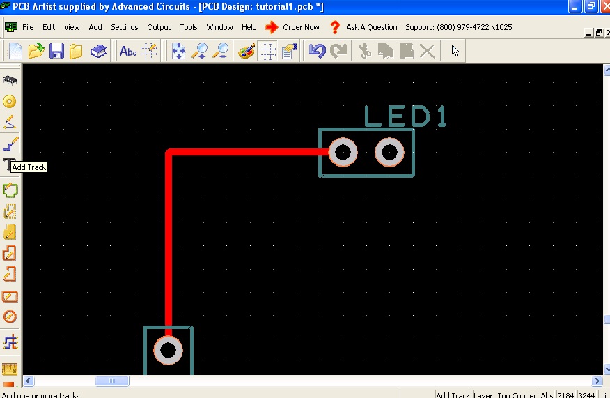
Select Add Track and connect the pins connected by the yellow line. Try to follow a convention, like a grid, to make things easier on more complicated boards. The default track width should be fine for most purposes. If there will be a lot of current flowing on the track, you should make it wider by right-clicking and choosing Properties. Tracks can be as wide as you want, within the spacing constraints. Ground tracks are often chosen to be as wide as possible. |
|||
====Standoffs ==== |
|||
[[Image:add_trace.jpg]] |
|||
Standoffs were used to attach the servo to the chassis and to attach the connector to the chassis. Two standoffs (1 in and 1/2 in) and several washers were used to make the connector parallel to the ground. |
|||
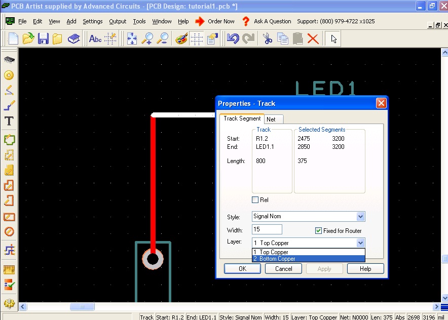
A good convention is to have traces running vertically be on one side of the board, and traces running horizontally be on the other. Select a portion of the trace, right click and select Properties. Here you can change the layer of the board and the width of the trace. |
|||
==== Passive Wheels ==== |
|||
[[image:Wheel.jpg|thumb|left|A Passive Wheel on the Dowel Pin]] |
|||
Passive wheels were mounted to the bottom of the chassis. Each wheel was made of a 3/4 inch pulley and an o-ring. The o-ring was used to increase friction with the ground. The wheels have been set on polished metal dowel pins which allow the wheels to rotate more freely than when placed on wooden dowels. The dowel pin axles were mounted (hot glue works but is not very strong) in the center of the segment. The center of the segment is not the center of the polycarbonate rectangle. Instead, the entire segment length is the distance from the standoff on one chassis to the center of the servo horn on the other. In this project, the length of the connector was made to be about half the length of the segment. Therefore, the wheels were placed at the same location as the stand off as can be seen in the image. The wheels are held in place with zip ties. |
|||
<br clear=all> |
|||
[[Image:edit_trace.jpg]] |
|||
==== Fully Assembled Body Segment ==== |
|||
[[image:BuiltChasis.jpg|thumb|right|A Chassis Built Showing a Standoff and Batteries]] |
|||
[[image:BuiltChasis2_MLS.jpg|thumb|right|Chassis with Batteries Removed]] |
|||
A fully assembled chassis has a mounted servo and is connected to a segment on either side. AAA batteries packs were attached to the sides of the motor with velcro to allow easy removal. The small electronic circuit board for each segment was mounted on the front of the motor to allow easy access to the switch. (See Electronic Design for more information on the circuit board and batteries) |
|||
<br clear=all> |
|||
Notice how the traces are automatically connected with a via to maintain connection. |
|||
=== The Head Segment === |
|||
[[image:BallCaster.jpg|thumb|left|The Ball Caster Under the Front Segment]] |
|||
[[Image:automatic_via.jpg]] |
|||
The head segment is similar to the body segments except that it contains a PCB board with a PIC instead of a servo motor. The head segment is the same width but slightly longer than the body segment. A ball caster was added to the front of the segment to help support the extra length and help the wheels stay on the ground. |
|||
<br clear=all> |
|||
Traces do not have to be drawn orthogonally. While drawing a trace, right click and select segment mode. These different modes will draw traces in a different way. Miter is the most common. |
|||
==== Protection and Visual Appeal ==== |
|||
[[image:Housing.jpg|thumb|right|One Segment of the Housing]] |
|||
[[Image:miter_trace.jpg]] |
|||
As a final step, housing for each segment was created from 3" PVC pipe. The pipe was cut into segments the same length as the chassis. The bottom of the pipe was cut off, allowing it to sit flat on the chassis. The housing provides a protective covering for the servo, batteries and electronics. The pipe was attached with velcro straps which mounted under the chassis. This housing can be easily removed to debug and to change batteries. |
|||
<br clear=all> |
|||
An orthogonally drawn trace can be turned into a miter by double clicking the corner and dragging the corner in. |
|||
=== Mechanical Debugging === |
|||
Use the Add Pad button and Add track to complete the circuit. You need to add these vias to make the power and ground connections because they do not translate from the Schematic Schema to the PCB. If you were to make this board, you would solder wires to these vias to supply power. |
|||
Wheels come off the ground: Add washers to the standoffs to force the chassis to be parallel to the ground. |
|||
[[Image:add_via.jpg]] |
|||
Wheels slide, but do not roll: Increase frictionby either adding weight to the segment or changing the "tires" (the o-ring). |
|||
Add some text reminders to the silkscreen layer to remind yourself where to solder the power and ground, what direction the LED goes, and what resistor to use. |
|||
<br clear=all> |
|||
[[Image:add_text.jpg]] |
|||
== Electronics == |
|||
====Parts List (Digikey Part Number)==== |
|||
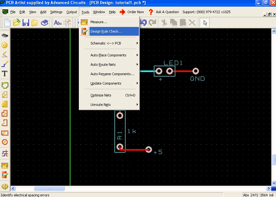
When your board is complete, use the Design Rule Check to automatically look for errors in connecting pins and accidentally crossed traces. You can check all the boxes. |
|||
*PIC: PIC18F4520 |
|||
*Oscillator: 40MHz Oscillator (X225-ND) |
|||
*RC Servo (see mechanical design) preferably high-torque |
|||
*10 wire IDC ribbon cable |
|||
*10 pos IDC cable socket (ASC10G): 1 per segment |
|||
*10 pos IDC cable header (A26267-ND): 1 per segment |
|||
*3 pos AAA battery holder (BH3AAA-W-ND): 1 per segment |
|||
*2 pos AAA battery holder (BH2AAA-W-ND): 1 per segment |
|||
*475 Ohm resistors (transmission line termination) |
|||
*Various switches to turn power electronics and the motors on/off |
|||
*Standard Protoboard, to mount connector from ribbon cable, and switches for each motor |
|||
*Xbee radio pair and PC |
|||
[[Image:design_rule_check.jpg]] |
|||
====Electronics in Each Body Segment==== |
|||
[[image:RibbonCable_schematic_HLS.jpg|thumb|right|Ribbon Cable Schematic]][[image:ServoBoard_schematic_HLS.jpg|thumb|right|ServoBoard Schematic]][[image:ServoBoard_Hooked_up_HLS.jpg|thumb|right|A Complete Circuit Board on the Snake]] |
|||
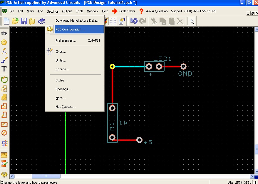
Go to Settings, PCB Configuration to make your board bigger or smaller or change other properties. You can also click on specific edges of your board to resize the board, or use the arrow to drag a box around all the components to select them and drag them around inside the board. |
|||
The each segment of the snake contains a Futaba Standard RC Servo. Each servo has 3 wires: power, ground, and signal. The signal generated by the microcontroller is carried by the IDC ribbon cable, and each servo board taps into a single signal line and the reference ground line as shown in the ribbon cable schematic. Each segment of the snake contains a small circuit board (ServoBoard Schematic) which has a connector for the ribbon cable, a switch to control the power, and a power indicator LED. Because of the length of the ribbon cable, each signal line must be terminated with a 475 ohm resistor to prevent reflected "ghost" signals from interfering with the original signal. |
|||
[[Image:pcb_config.jpg]] |
|||
Each servo board also has its own power supply of 5 AAA cells, which gives each servo 7.5V. Although the servos are only rated for 6V, 7.5V was used because more torque was needed. The current drain (up to 500mA) caused the voltage across the cells to drop due to the high internal resistance of the alkaline cells. NiMH rechargeable cells are more capable of handling high current draw applications, but are also much more expensive and can take several hours to charge. |
|||
Use this document, [[Media:Student Order Process updated 4-14.pdf|Student Order Process]], to purchase a board with the $33 Student Discount. (Maximum board size for this special is 60 square inches.) |
|||
The robot snake can run for about 1 hour on the alkaline cells, after which the servos no longer have enough torque to generate the serpentine motion. |
|||
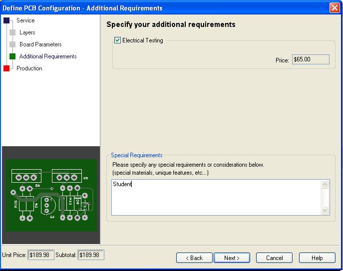
Go back to PCB Configuration and Enter Student in the Special Requirements section. |
|||
<br clear=all> |
|||
[[Image:student_order.jpg]] |
|||
====Electronics in The Head Segment==== |
|||
[[image:PICBoard_schematic_HLS.jpg|thumb|right|The Mainboard Schematic]] |
|||
[[image:PICBoard_HLS.jpg|thumb|right|The Electronics in the Head]] |
|||
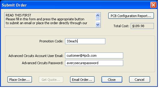
Go to Output, Submit Order. PCB Artist will perform a Design Rule Check. After that, enter the Promotion Code 33each. If you do not have an Advanced Circuits account, go to [http://www.4pcb.com 4pcb.com] and make one. Then you may order your board. |
|||
The PIC18F4520 Prototyping Board designed by Professor Peshkin was used. Schematics of the board can be found here: [[Main_Page#PIC_18F4520_prototyping_board|18F4520_prototyping_board]]. The only change applied to the board was to replace the 20MHz clock with a 40MHz clock. This allowed the microcontroller to perform calculations faster, improving the resolution of the servo signal. The ribbon cable was connected to the ground and port D pins on the PIC. |
|||
[[Image:submit_order.jpg]] |
|||
An [[XBee_radio_communication_between_PICs|XBee radio]] was used to communicate between the microcontroller and the PC. The wiring diagram shows a schematic for the Xbee connection with the PIC. The [[XBee_radio_communication_between_PICs#XBee_Interface_Module|XBee Interface Board]] was used to provide a robust mechanical mount for the radio, as well as supply the 3.3V needed by the XBee. On the PC side, another XBee interface board was plugged into the FTDI USB-Serial converter. Other than this, no special electronics were needed for the XBee radio. The radio simply acted as a serial cable replacement The snake was controlled by sending commands with a terminal program. |
|||
==Adding a Component to the Library== |
|||
<br clear=all> |
|||
A majority of the time the component you want to use is not in the existing libraries, therefore, you have to create a component. A component consists of a schematic symbol, a pcb symbol and a mapping between the pins of the schematic symbol and the pcb symbol. This section details how to create a component using the SN74HC04 Hex Inverter as an example. |
|||
== PIC Code == |
|||
There are two PIC files used in this robotic snake, SnakeServos.c and main.h, which are shown below. main.h sets up the default parameters used in SnakeServos.c. The microcontroller controls the RC servos and receives data from a computer via serial communication. |
|||
===Create a Schematic Symbol=== |
|||
The main purpose of SnakeServos.c is to calculate the motion profile of the servos, and send a corresponding signal to each of the servos every 20 ms. The code for this is found in the <tt>ISR_20MS</tt> function in the code which is run every 20ms. |
|||
With PCBArtist open (it doesn't matter if any schematics or pcb files are open), click on the blue book at the top of the screen. |
|||
A secondary function is to update the parameters that affect the motion of the snake. The code for this can be found in the <tt>ISR_USART_RX</tt> function, which is run every time a byte is received on the USART's receive buffer. |
|||
[[Image:PCBArtist_BlueBook.jpg]] |
|||
====Servo Control Details==== |
|||
<br clear=all> |
|||
The main function of the PIC microcontroller is to control multiple RC servos (seven in our case). See [[RC Servo Theory]] for a discussion of the control signal for an RC servo. The RC servo expects a pulse every 20ms, so a timer called Timer1 is set up to overflow every 20 ms and trigger an interrupt. When the interrupt is triggered, the counter for Timer1 is set to the value held by the constant <tt>TMR1_20MS</tt> (defined as <tt>15536</tt>), which will cause Timer1 to overflow 20 ms later and re-trigger the interrupt. |
|||
This opens the Library Manager of schematic symbols, pcb symbols and components. It will look something similar to the image below. |
|||
[[Image:PCBArtist_LibraryManager.jpg]] |
|||
As shown in the RC Servo Theory, the width of the high pulse determines the angle of the servo. As a result, the pulse width corresponding to the desired angle for each servo motor is calculated and the corresponding timer value is stored in an array called <tt>RCservo</tt>. At the beginning of the interrupt, all the pins connected to the servos are set high. For the RC servos used in this project, the maximum pulse width can be 2.25 ms; therefore, <tt>Timer1</tt> only needs to be polled for 2.25 ms. <tt>TMR1_2point25MS</tt> is a constant corresponding to the value of <tt>Timer1</tt> 2.25 ms after the interrupt begins and is defined as <tt>15536 + 6250</tt>. While <tt>Timer1</tt> is less than this variable, the counter is compared sequentially to the values in the <tt>RCservo</tt> array plus 15536 (15536 must be added because the Timer1 started counting at 15536 instead of 0). Since the <tt>RCservo</tt> array corresponds to the pulse widths of the servos, when the value of <tt>Timer1</tt> is greater than a value in <tt>RCservo</tt> plus 15536, the corresponding pin is set low. After the sequence is complete, <tt>Timer1</tt> is polled again and the process repeats until 2.25 ms have elapsed, which corresponds to when Timer1 is greater than <tt>TMR1_2point25MS</tt>. After all the servo signals have been sent, the values in the <tt>RCservo</tt> array are updated to prepare for the next 20ms interrupt. |
|||
<br clear=all> |
|||
To make a component, we first need to download the datasheet of the component. Download the datasheet for the Hex Inverter [[Media:SN74HC04Inverter.pdf|here]]. |
|||
Although polling the timer to control the length of a pulse has a lower resolution than using an interrupt (see [http://peshkin.mech.northwestern.edu/pic/code/RCservoSoft/RCservoSoft.c RCservoSoft.c]), it allows one to add and remove servos more easily and not have to decrease the frequency of the servo signal pulse train. With a 40MHz clock and seven servos, the resolution for the pulse was about 8us, which was sufficient for this project. |
|||
<br clear=all> |
|||
On the first page of the datasheet, we can find a schematic of the component for SN74HC04. We will use this schematic to make our schematic in PCB Artist. |
|||
====Serial Communication Details==== |
|||
*In PCBArtist, click on the 'Schematic Tab' of the Library Manager. |
|||
The PIC communicates serially with a XBee radio to a PC with a XBee radio. As shown in the code, the serial communication allows the user to change the speed, the amplitude and period of the sine wave, and the direction (forward, reverse, left and right) of the robotic snake. When a byte is received in the UART receive buffer, a high-priority interrupt is triggered. The received byte is put into a switch-case statement, and the corresponding parameters are updated. |
|||
*Click on the 'Wizard' Button in the middle of the window to begin creating a schematic symbol. |
|||
This wizard will help you make your schematic symbols. |
|||
====SnakeServos.c==== |
|||
*Click 'Next' |
|||
<pre> |
|||
[[Image:PCBArtist_Sch_Start.jpg]] |
|||
/* |
|||
<br clear=all> |
|||
Andy Long, Clara Smart, and Michael Hwang's snake robot code. |
|||
*/ |
|||
*Choose English with a precision of 1 (these are the units for the symbol) |
|||
*Click 'Next' |
|||
[[Image:PCBArtist_Sch_Tech.jpg]] |
|||
<br clear=all> |
|||
*Next we are going to choose the type of symbol. Our chip has pins on two sides so select the rectangle with pins on two sides (the first one). |
|||
#include <18f4520.h> |
|||
*Select the 'center' option for Origin. If you decide to rotate the symbol, it will rotate about this point. |
|||
#device high_ints=TRUE // this allows raised priority interrupts, which we need |
|||
*Select the top left corner for Component Name. This indicates where the component name will be placed. |
|||
#fuses HS,NOLVP,NOWDT,NOPROTECT |
|||
*Click 'Next' |
|||
#use delay(clock=40000000) |
|||
[[Image:PCBArtist_Sch_SymbolType.jpg]] |
|||
#use rs232(baud=9600, UART1) |
|||
<br clear=all> |
|||
*In the next window, you can choose how you want the pins to be represented, the size of these and the length of the lines going to the pins. Leave these with the default values. |
|||
#include <main.h> |
|||
*Click 'Next' |
|||
#include <math.h> |
|||
[[Image:PCBArtist_Sch_Styles.jpg]] |
|||
<br clear=all> |
|||
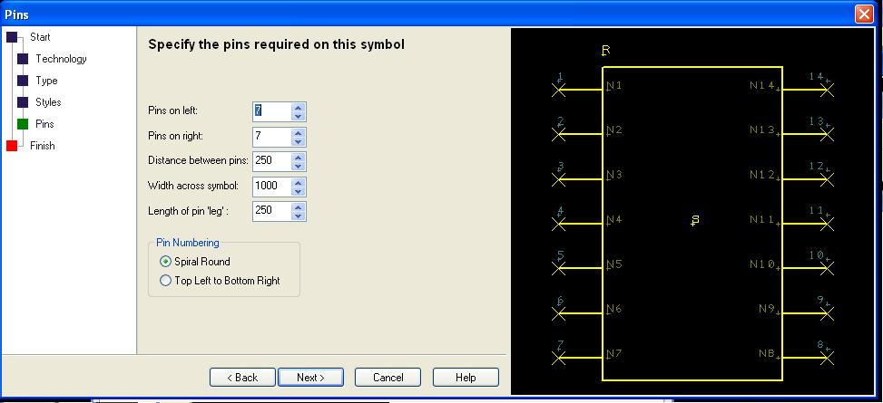
The next window determines the number of pins on each side of the component and some dimensions. |
|||
*Enter 7 for both Pins on left and Pins on Right. |
|||
*The other dimensions are not as important for the schematic, leave these as the default. (They can be editted later if too big or too small). |
|||
*The last part on this page describes how the pins are numbered. Since the schematic on the datasheet spirals the numbers, select the 'Spiral Round' option. |
|||
*Click 'Next' |
|||
[[Image:PCBArtist_Sch_Pins.jpg]] |
|||
<br clear=all> |
|||
The last window is where you name the symbol and save it to a specific library. |
|||
/* |
|||
*Name the component SN74HC04_Inverter and save it in the ME333_Lab2 Library that you downloaded above. |
|||
Put your desired high duration here; |
|||
*Click Finish |
|||
3200 is center |
|||
You have now created a schematic symbol. If you checked the 'Edit the symbol now' box, you can see the schematic and edit if you want. We won't do any editting right now though. |
|||
1000 is 90 deg right |
|||
[[Image:PCBArtist_Sch_Finish.jpg]] |
|||
5400 is 90 deg left |
|||
<br clear=all> |
|||
*/ |
|||
int16 RCservo[7]; |
|||
===Create a PCB Symbol=== |
|||
//use volatile keyword to avoid problems with optimizer |
|||
The next step is to create a pcb symbol for the component. This will be the footprint on your PCB. Look at the datasheet again and find the Plastic Dual-In Line Package footprint for the SN74HC04 (page 10). This tells us the dimensions we need for our footprint. |
|||
volatile float a = A_DEFAULT; |
|||
volatile float b = B_DEFAULT; |
|||
volatile float c = C_DEFAULT; |
|||
*Click on the Library Manager (blue book). |
|||
volatile float alpha; |
|||
*Go to the PCB Symbols tab. |
|||
volatile float gamma; |
|||
*Click on the Wizard again. |
|||
volatile float beta; |
|||
*Click Next on the start up window. |
|||
volatile float speed = 0; |
|||
*On the Technology window, choose English with 'thou' as the unit and precision of 1. We choose this because it is the smallest unit on the datasheet for the English units. |
|||
volatile float prev_speed = SPEED_DEFAULT; |
|||
float t = 0; |
|||
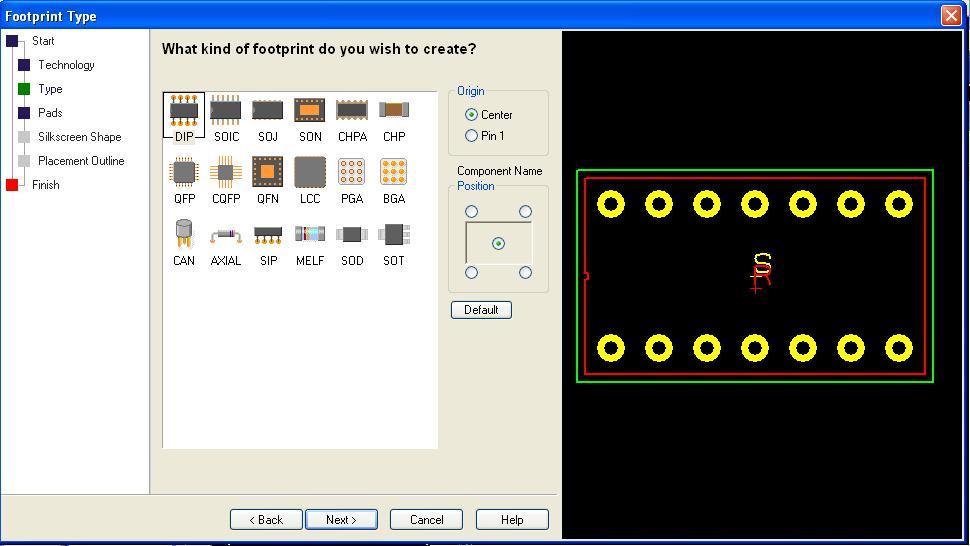
The next window is the footprint type. |
|||
#INT_TIMER1 // designates that this is the routine to call when timer1 overflows |
|||
* Select DIP type (the top left). |
|||
//generates servo signals |
|||
* For Origin - select center |
|||
void ISR_20MS(){ |
|||
* For Name - select center - this is where the name will be displayed on the PCB |
|||
volatile unsigned int16 time; |
|||
*Click 'Next' |
|||
set_timer1(TMR1_20MS); //set timer to trigger an interrupt 20ms later |
|||
[[Image:PCBArtist_PCB_FootPrint.jpg]] |
|||
SET_ALL_SERVOS(0b11111111); //begin pulse for servo signal |
|||
<br clear=all> |
|||
time=get_timer1(); //poll timer |
|||
while(time < TMR1_2point25MS){ //end this loop after 2.25 ms |
|||
if (time > (RCservo[0] + TMR1_20MS)){ |
|||
output_low(SERVO_0); //end the pulse when time is up |
|||
} |
|||
if (time > (RCservo[1] + TMR1_20MS)){ |
|||
output_low(SERVO_1); |
|||
} |
|||
if (time > (RCservo[2] + TMR1_20MS)){ |
|||
output_low(SERVO_2); |
|||
} |
|||
if (time > (RCservo[3] + TMR1_20MS)){ |
|||
output_low(SERVO_3); |
|||
} |
|||
if (time > (RCservo[4] + TMR1_20MS)){ |
|||
output_low(SERVO_4); |
|||
} |
|||
if (time > (RCservo[5] + TMR1_20MS)){ |
|||
output_low(SERVO_5); |
|||
} |
|||
if (time > (RCservo[6] + TMR1_20MS)){ |
|||
output_low(SERVO_6); |
|||
} |
|||
time=get_timer1(); //poll timer |
|||
} |
|||
SET_ALL_SERVOS(0); //set all servos low in case some pins are still high |
|||
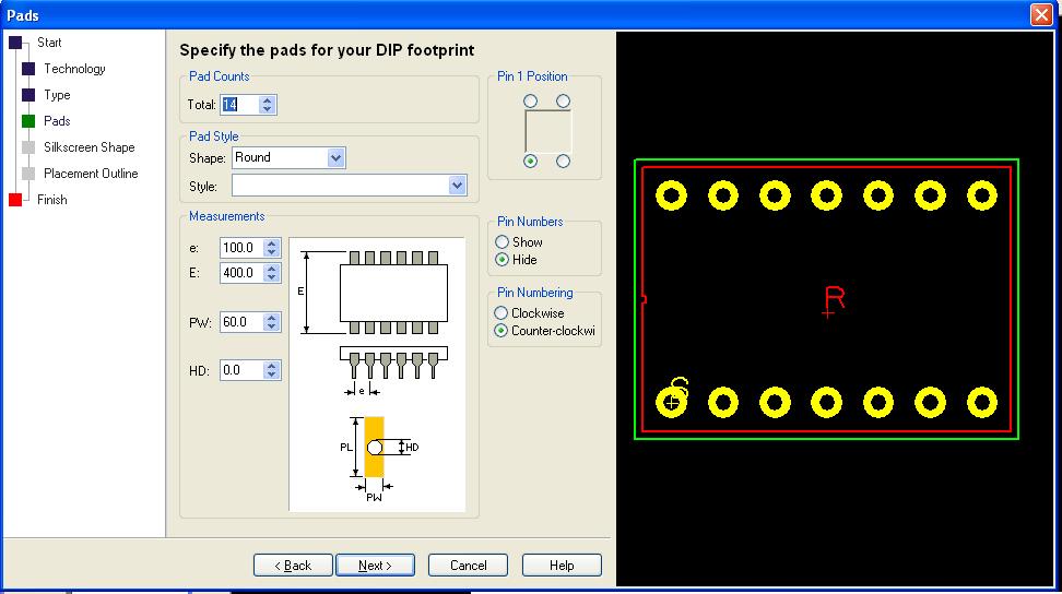
The next window describes the pads on the PCB. This window will be different for the different types of chips. |
|||
//3200 is center //1000 is 90 deg right // 5400 is 90 deg left |
|||
*Choose 14 pads |
|||
/* |
|||
*For the Pad Style, choose 'Round' and leave Style blank. |
|||
add value of sine wave with phase offset ((alpha*sin(t + X*beta), |
|||
The units are in thousands of inches |
|||
3200 for servo center position, |
|||
*e = 100 for 0.1 in pitch (as shown on the datasheet). |
|||
an adjustment value to compensate for offsets when mounting servo horn (SERVO_X_ADJ), |
|||
*E = 400. We can put this value between 325 and 430 as shown on the datasheet, but we also know that the chip can plug into a breadboard (spacings of 0.1 in), so 400 thou is a good number. |
|||
and bias (gamma) for turning. |
|||
*PW = 60 and HD = 30. HD refers to the hole diameter for the pin. The pin diameter is around 20 thou as shown on the datasheet, so 30 thou is a good number with extra space. PW is the pad width (extra copper) surrounding the hole. Extra 30 thou is generally a good pad width. |
|||
*/ |
|||
*Choose Pin 1 Position to be the lower left corner (same as in the footprint on the datasheet) |
|||
RCservo[0]=(int16)(alpha*sin(t) + 3200 + SERVO_3_ADJ + gamma); |
|||
*We don't want the pin numbers to be displayed on the PCB so select Hide for the Pin Numbers |
|||
RCservo[1]=(int16)(alpha*sin(t + 1*beta) + 3200 + SERVO_4_ADJ + gamma); |
|||
*Pin number is counter clockwise. |
|||
RCservo[2]=(int16)(alpha*sin(t + 2*beta) + 3200 + gamma + SERVO_5_ADJ); |
|||
*Click Next |
|||
RCservo[3]=(int16)(alpha*sin(t + 3*beta) + 3200 + gamma + SERVO_6_ADJ); |
|||
[[Image:PCBArtist_PCB_Pads.jpg]] |
|||
RCservo[4]=(int16)(alpha*sin(t + 4*beta) + 3200 + gamma + SERVO_7_ADJ); |
|||
<br clear=all> |
|||
RCservo[5]=(int16)(alpha*sin(t + 5*beta) + 3200 + gamma + SERVO_8_ADJ); |
|||
RCservo[6]=(int16)(alpha*sin(t + 6*beta) + 3200 + gamma + SERVO_9_ADJ); |
|||
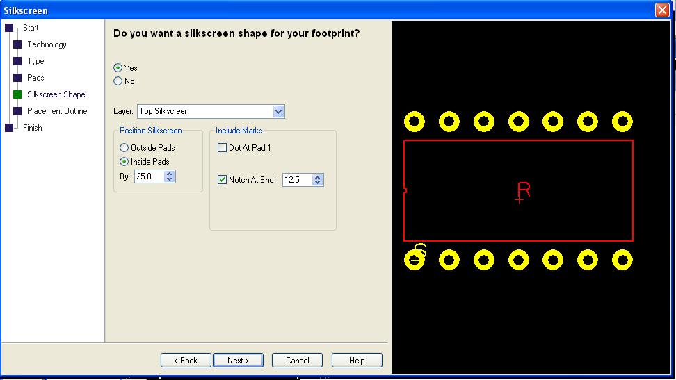
The next window describes the silk screen (the writing on top of the PCB). |
|||
t+= speed; //increment time, wrap around if necessary to prevent overflow |
|||
*Click Yes |
|||
if (t > 2*pi){ |
|||
*Layer - Top Silkscreen |
|||
t = 0; |
|||
*Inside pads by 25 (sometimes you may want the silk screen to be outside the pads, but it is really your choice) |
|||
} |
|||
*Include Marks - Notch at end (12.5) --> this helps you figure out the orientation of the component |
|||
else if (t < 0){ |
|||
*Click Next |
|||
t = 2*pi; |
|||
[[Image:PCBArtist_PCB_SilkScreen.jpg]] |
|||
} |
|||
} |
|||
<br clear=all> |
|||
The next window asks if you want a placement shape (rectangle) around the entire component. We are not going to include this. |
|||
*Click No |
|||
*Click Next |
|||
*On the final window, name it SN74HC04_Inverter (same name as the schematic) and save it in the ME333 Library. |
|||
#INT_RDA HIGH //High-Priority Interrupt triggered by USART Rx |
|||
*Click Finish |
|||
//parameter update |
|||
void ISR_USART_RX(){ |
|||
char input; |
|||
if (kbhit()){ |
|||
input = getc(); |
|||
switch(input){ |
|||
case 'w': //accelerate |
|||
speed += 0.002; |
|||
break; |
|||
case 's': //decelerate |
|||
speed -= 0.002; |
|||
break; |
|||
case 'x': //pause motion |
|||
prev_speed = speed; |
|||
speed = 0; |
|||
break; |
|||
case 'z': //resume motion |
|||
speed = prev_speed; |
|||
break; |
|||
case 'c': //reverse speed |
|||
speed = -speed; |
|||
break; |
|||
case 'a': //increase left turn rate |
|||
c -= 1000; |
|||
gamma=-c/num_segments; |
|||
break; |
|||
case 'd': //increase right turn rate |
|||
c += 1000; |
|||
gamma=-c/num_segments; |
|||
break; |
|||
case 'f': //set turn rate to 0 |
|||
c = C_DEFAULT; |
|||
gamma = 0; |
|||
case 't': //increase amplitude |
|||
a += 10; |
|||
alpha=a*abs(sin(beta)); |
|||
break; |
|||
case 'g': //decrease amplitude |
|||
a -= 10; |
|||
alpha=a*abs(sin(beta)); |
|||
break; |
|||
case 'y': //increase phases in body |
|||
b += 0.1; |
|||
beta=b/num_segments; |
|||
alpha=a*abs(sin(beta)); |
|||
break; |
|||
case 'h': //decrease phases in body |
|||
b -= 0.1; |
|||
beta=b/num_segments; |
|||
alpha=a*abs(sin(beta)); |
|||
break; |
|||
case '1': //preset 1 |
|||
a = A_DEFAULT; |
|||
b = B_default; |
|||
c = C_default; |
|||
gamma=-c/num_segments; |
|||
beta=b/num_segments; |
|||
alpha=a*abs(sin(beta)); |
|||
speed=SPEED_DEFAULT; |
|||
break; |
|||
case '2': //preset 2 |
|||
a = 1400; |
|||
b = 2*pi; |
|||
c = C_DEFAULT; |
|||
gamma=-c/num_segments; |
|||
beta=b/num_segments; |
|||
alpha=a*abs(sin(beta)); |
|||
speed=SPEED_DEFAULT; |
|||
break; |
|||
case '3': //preset 3 |
|||
a = 1000; |
|||
b = 5*pi; |
|||
c = C_DEFAULT; |
|||
gamma=-c/num_segments; |
|||
beta=b/num_segments; |
|||
alpha=a*abs(sin(beta)); |
|||
speed=SPEED_DEFAULT; |
|||
break; |
|||
default: |
|||
} |
|||
} |
|||
return; |
|||
} |
|||
You have now created a PCB footprint. |
|||
void main() { |
|||
//load default values |
|||
a = A_DEFAULT; |
|||
b = B_default; |
|||
c = C_default; |
|||
gamma=-c/num_segments; |
|||
beta=b/num_segments; |
|||
alpha=a*abs(sin(beta)); |
|||
speed=0; |
|||
setup_timer_1(T1_INTERNAL | T1_DIV_BY_4 ); |
|||
set_timer1(0); |
|||
enable_interrupts(INT_TIMER1); //enable Timer1 interrupt |
|||
enable_interrupts(INT_RDA); //enable USART receive interrupt |
|||
enable_interrupts(GLOBAL); |
|||
while (TRUE) { |
|||
<br clear=all> |
|||
} |
|||
} |
|||
</pre> |
|||
=== |
===Create a Component=== |
||
We created a schematic symbol and a pcb symbol above. Now we are going to create a component to link the two symbols. |
|||
<pre> |
|||
#ifndef __MAIN_H__ |
|||
#define __MAIN_H__ |
|||
*Click on the Library Manager and go to the Component tab. |
|||
#define SET_ALL_SERVOS(x) output_d(x) |
|||
*Click on the Wizard button |
|||
*Click Next on the opening window |
|||
The first window allows you to select what type of component you are making. You can make a Normal Component (both Schematic and PCB), only a Schematic component or only a PCB component. |
|||
/* |
|||
*Select Normal Component |
|||
This chart matches the pin on the PIC to the wire on the ribbon cable |
|||
*Click Next |
|||
PIN WIRE IN USE |
|||
--- ---- ------- |
|||
RD0 2 |
|||
RD1 3 * |
|||
RD2 4 * |
|||
RD3 5 * |
|||
RD4 6 * |
|||
RD5 7 * |
|||
RD6 8 * |
|||
RD7 9 * |
|||
This windows contains the details for the component. |
|||
*/ |
|||
*Name = SN74HC04_Inverter (same as the symbols) |
|||
#define SERVO_3_ADJ 0 |
|||
*Package - type DIP (this really doesn't matter) |
|||
#define SERVO_4_ADJ 300 |
|||
*Default Reference - choose IC for integrated circuit |
|||
#define SERVO_5_ADJ (-150) |
|||
*Component pins - 14 |
|||
#define SERVO_6_ADJ 75 |
|||
*Number of Gates - 1 - this is the number of times your schematic symbol is needed for the component |
|||
#define SERVO_7_ADJ (-200) |
|||
*Click Next |
|||
#define SERVO_8_ADJ 100 |
|||
[[Image:PCBArtist_Component_Details.jpg]] |
|||
#define SERVO_9_ADJ (-150) |
|||
<br clear=all> |
|||
In the next window you select the schematic symbol that you want to use |
|||
#define SERVO_0 PIN_D1 |
|||
*Select SN74HC04_Inverter from the ME333 Library |
|||
#define SERVO_1 PIN_D2 |
|||
*Click Next |
|||
#define SERVO_2 PIN_D3 |
|||
In the PCB window, you select the pcb symbol that you want to use |
|||
#define SERVO_3 PIN_D4 |
|||
*Select SN74HC04_Inverter from the ME333 Library |
|||
#define SERVO_4 PIN_D5 |
|||
*Click Next |
|||
#define SERVO_5 PIN_D6 |
|||
#define SERVO_6 PIN_D7 |
|||
The next window assigns the pins from the schematic to the pcb. |
|||
#define A_DEFAULT 1300 |
|||
Since we choose our pins in the schematic and pcb to have the same order: |
|||
#define B_DEFAULT 3*pi |
|||
*Select Assign 1-to-1 button to assign Pin 1 Schematic to Pin 1 PCB ... etc |
|||
#define C_DEFAULT 0 |
|||
We can also choose to add names to each pin. |
|||
*Assign the pins names (1A,1Y,GND..etc) to each of the pins as shown on the datasheet. |
|||
#define SPEED_DEFAULT 0.05 |
|||
*Click Next |
|||
#define OMEGA_DEFAULT 1 |
|||
[[Image:PCBArtist_Component_Pins.jpg]] |
|||
#define num_segments 8 |
|||
<br clear=all> |
|||
#define TMR1_20MS 15536 |
|||
#define TMR1_2point25MS 15536 + 6250 |
|||
#endif |
|||
</pre> |
|||
== Results == |
|||
Overall, the robotic snake was successful. |
|||
Initially, the mechanical design included a single wheel mounted in the center of the pvc pipe. However, the motion of the snake was very difficult to control because the robotic snake became unstable very easily. As a result, the chassis was built to include two wheels, as discussed in the mechanical design section, in order to provide stability which made the robot easier to control. |
|||
Wireless control from a laptop allowed easy demonstration of the snakes capabilities, and allowed others to easily control its movement. |
|||
The final robotic snake can be seen in action here. |
|||
[http://www.youtube.com/watch?v=Sb8WqaLX1Vo Video of the robot snake without housing] |
|||
[http://www.youtube.com/watch?v=r_GOOFLnI6w Video of the robot snake with housing] |
|||
== Next Steps == |
|||
The robotic snake was developed within five weeks, and proved to be a very successful demo. There are many options that could be researched and developed to add to this robot and discussed below. |
|||
==== Position Sensors ==== |
|||
Sensors could be added to the robot to allow it to know its position. This could be accomplished with a combination of encoders on a segment. Most likely, the middle segment should be used since it would be the approximate center of gravity. Knowledge of the position of the center of gravity would potentially the robotic snake to be sent to different locations or navigate (using dead reckoning) through a pre-determined obstacle course or maze. The information from encoders could be sent to a computer to observe different snakelike motions with different parameters. |
|||
==== Obstacle Avoidance ==== |
|||
With optical sensors on the head of the snake, the robot would be able to sense an obstacle and either overide the wireless command and avoid it, or stop completely, and wait for further commands. |
|||
==== Power Supply ==== |
|||
Currently, 5 AAA batteries are required for each servo, meaning that this robot requires many batteries. As a result, a different power supply could be investigated. |
|||
====High Torque Servos==== |
|||
The servos in the snake have a large load but do not need to move very quickly, so high torque servos could be used instead of standard servos. This would also prolong the battery life because the servos would be operating in a more efficient range. |
|||
On the final window: |
|||
== References == |
|||
*Click Save the component to the library --> Put it in the ME333 library |
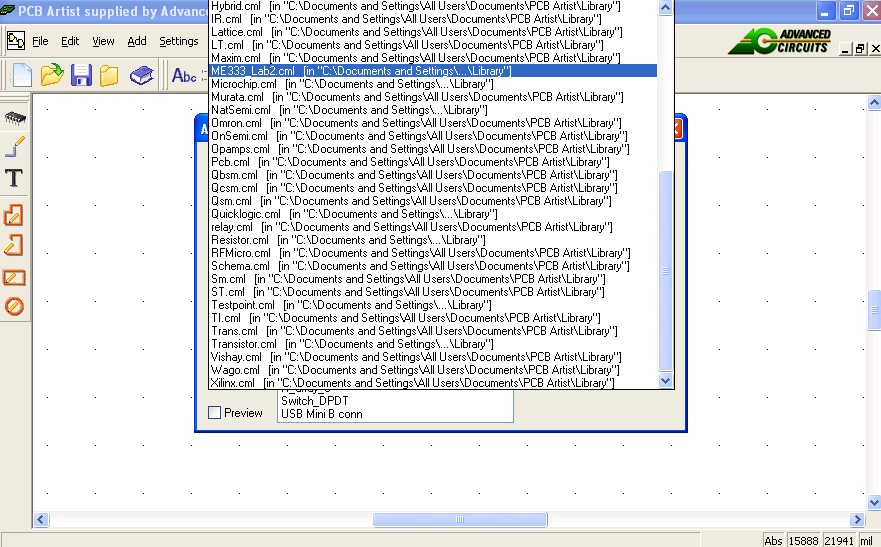
|||
If you want to edit the component now (check the next box) |
|||
*Click finish |
|||
You have now created a component and can use it with schematics and pcbs. |
|||
Ma, Shugen. "Analysis of creeping locomotion of a snake-like robot." ''Advanced Robotics'' Vol 15, No 2 (2001): 205-6. |
|||
== Practice Making a PCB == |
|||
Saito, Fukaya, Iwasaki. "Serpentine Locomotion with Robotic Snakes". ''IEEE Control Systems Magazine'' (Feb 2002): 66, 72-73. |
|||
After reviewing this tutorial, you are ready to [[Practice Making a PCB]]. |
|||
Latest revision as of 16:01, 13 January 2010
What is a PCB?
A printed circuit board, or PCB, is an epoxy board clad with copper sheets to make electrical connections along fixed routes. A PCB can have many layers of copper and insulator, depending on the complexity of the design. Layers are connected with vias, plated holes maintaining electrical conductivity. A finished PCB is often covered with solder mask, a solder-phobic layer that helps prevent solder bridges, making the PCB green. A white silk screen can be drawn on top of this, used to label the outlines of components and give other critical information. For more information on PCBs, see the wikipedia page Printed Circuit Board.
PCBs are created in a variety of ways. A common method is covering the copper you wish to keep and dipping the board in acid, which etches away the copper you do not want. This method can be done by hand.
A more professional and reliable PCB can be made by designing your circuit in CAD software and ordering the part from a PCB production house. The remainder of this page will describe how to use the proprietary software PCB Artist to design and order a complete PCB.
Advanced Circuits and PCB Artist
Advanced Circuits (www.4pcb.com) is a company based in Colorado known for their quick turn-around and good prices on low volume printed circuit board (PCB) orders. This is the main supplier for PCBs created by students for clases or research at Northwestern.
Previously, the PCB was created in TraxxMaker or other CAD PCB program, many of which are outdated and difficult to use, then uploaded to Advanced Circuits. Advanced Circuits has created PCB Artist, free software to create schematics and PCBs. This software is designed to order only from Advanced Circuits. This somewhat simplistic software is very intuitive (once comfortable) and allows for simple changes and editing. Additionally, the component library offered is up to date and contains many specific components. This Wiki page will cover the development and ordering process of a simple PCB board.
Contact at Advanced Circuits
Jackie Sartin - Regional Sales Manager
E-mail: jackies@4pcb.com Call: 1-800-979-4PCB (4722) Ext: 1685
Getting Set Up
- Have a complete circuit schematic and know exactly what parts (including part numbers) you are using.
- Download the software Or, type “PCB Artist” into google. Then click the download button in the middle of the screen.
- Review the material on this page: Help Guides and User Reference documents
Browse through the Advanced Circuits tutorial pdf to get familiar with the program interface and design process. In general, you will:
- Create a schematic (.sch) that represents the circuit you want to create. This schematic is just like any other schematic you would draw by hand, but it will be used to automate the process of laying out your physical PCB and is very helpful in debugging.
- Create a PCB design (.pcb) that represents your physical PCB, based on your schematic. In this CAD process, the program will automatically grab the components you need and place them outside of the board. You then place each component and connect the pins based on how they are connected in the schematic. The program helps you by highlighting the nets (all the pins that need to be connected) in different colors. You choose how to connect each pin, the width of the copper trace, the layer the copper should be on (top or bottom for a 2 sided board), and the size of the vias. You can have PCB Artist automatically place your components and connect them, but the result may not be pretty or successful.
- Check for errors. Use the Design Rule Check tool to make sure the board is machinable and the pins are connected as they are in your schematic. Carefully scan your board to make sure vias don't accidentally touch traces. Put some silk screen labels next to pins and components, and put your name and the version of your board somewhere for later reference.
- Order your board! Use the student deal ($33 for one board), but note it generally takes a week to make and a few days to ship (another $15). So order early and design carefully.
Some general tips:
- Don't try to make a 2" x 2" board if your space constraints allow for a larger board. It is not worth the effort and possible mistakes trying to squeeze everything into a tiny area if you don't have to.
- Connect your power and ground traces first, they are usually the most complicated.
- Try to keep an organized board. Keep components with many connections close together.
- Use a convention like top layer traces go left-right and bottom layer traces go up-down, this will make routing much easier.
- Give yourself some prototyping area and add extra vias to traces. Thus will allow you some wiggle room when your board arrives and has errors (every board will have some errors!). Traces can be cut with a razor blade fairly easily if the board is not too tight, and can be remade with wires if you remember to leave some extra vias around to solder to.
Download and Installation Instructions
Download and install PCB Artist from Advanced Circuits at the Advanced Artist website. The latest version as of 1/7/2010 is 1.3.2. It is PC only and works best in Windows XP.
To install a library, download the example .zip file here. Extract the files and place them in the PCB Artist Library folder. On Windows XP the default location is: C:\Documents and Settings\All Users\Documents\PCB Artist\Library, and on Windows Vista or Windows 7 the default location is C:\Users\Public\Documents\PCB Artist\Library.
Create a Schematic
Open a new schematic.
Select Add a Component.
Choose the library your component is in (the ME333 library).
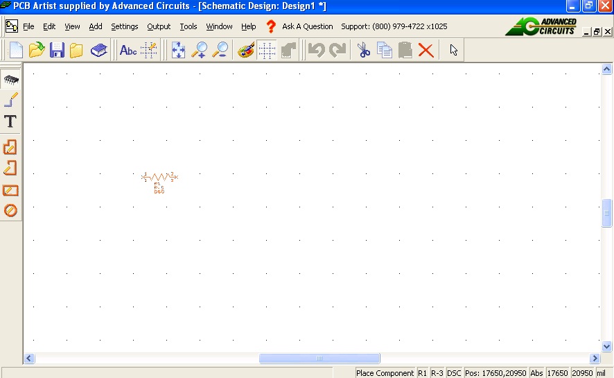
Place the component R-3. Components should be arranged so that the schematic can be read and understood easily, they do not need to be laid out as they would on the PCB, we will do that later. To drag components around in the schematic, click the arrow button in the toolbar at the top to get the arrow cursor.
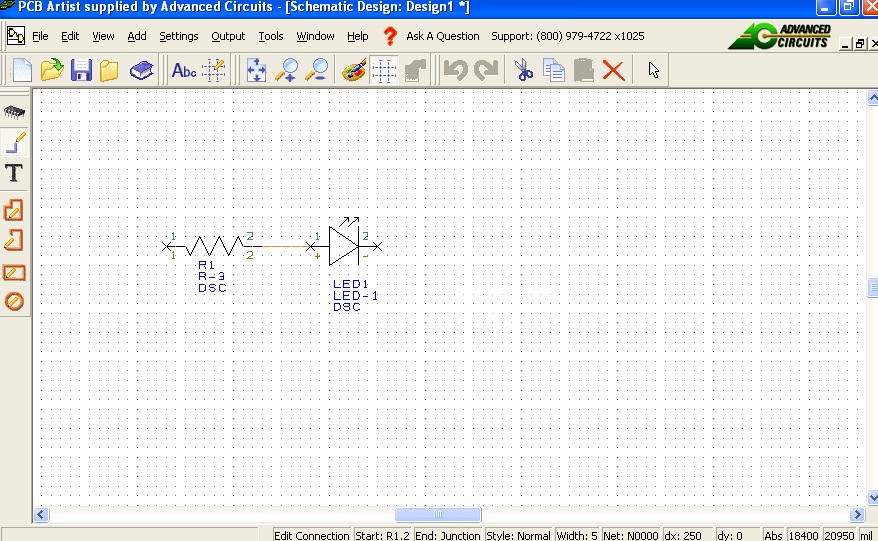
Add the LED from the ME333 library and connect the components using the Add Schematic Connection tool (the icon on the left that looks like a pencil drawing a line). Such connections will make it easier to create the PCB. They indicate which pins need to be connected on the PCB, but they do not represent the actual paths the traces will take. We will design those later.
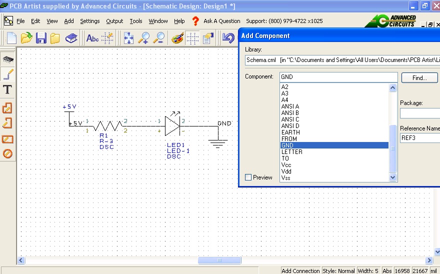
Add a voltage source and ground from the Schema library and connect them to the schematic.
Save the file (.sch). Now we can design a PCB for this circuit.
Create PCB from Schematic
Open your schematic and go to Tools, Schematic <--> PCB, Translate to PCB.
Go through the New PCB Wizard, selecting your board size or defining a custom size. This can always be changed later if you need a larger or smaller board.
Use a 2 layer board with the default properties. At this screen,
do not enter anything, but later we will add a comment to allow us to buy a Student discount board for $33 plus shipping.
Enter a board number and revision number. Use a 1 week turn around with 1 unit. Ignore the cost, that will change to $33 later.
Have the program place the components outside of your board so you can arrange them where you want them.
Translate the components to the inside of the green box which represents the outline of your board. Rotate a component by right clicking on the part and choosing rotate. All of the components must be moved inside of the green box to finish the board. These will be their locations on the board.
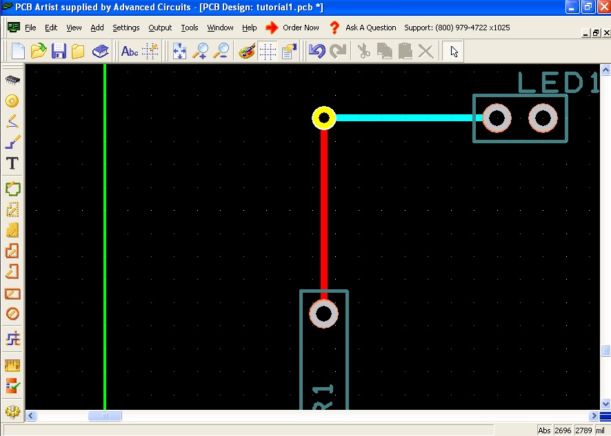
Select Add Track and connect the pins connected by the yellow line. Try to follow a convention, like a grid, to make things easier on more complicated boards. The default track width should be fine for most purposes. If there will be a lot of current flowing on the track, you should make it wider by right-clicking and choosing Properties. Tracks can be as wide as you want, within the spacing constraints. Ground tracks are often chosen to be as wide as possible.
A good convention is to have traces running vertically be on one side of the board, and traces running horizontally be on the other. Select a portion of the trace, right click and select Properties. Here you can change the layer of the board and the width of the trace.
Notice how the traces are automatically connected with a via to maintain connection.
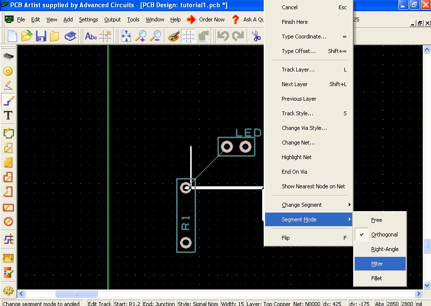
Traces do not have to be drawn orthogonally. While drawing a trace, right click and select segment mode. These different modes will draw traces in a different way. Miter is the most common.
An orthogonally drawn trace can be turned into a miter by double clicking the corner and dragging the corner in.
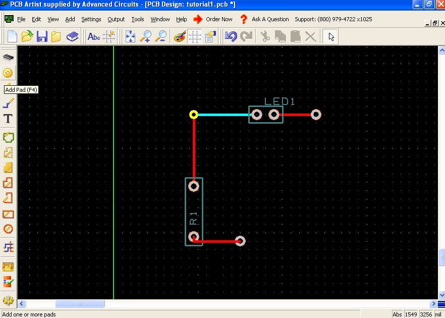
Use the Add Pad button and Add track to complete the circuit. You need to add these vias to make the power and ground connections because they do not translate from the Schematic Schema to the PCB. If you were to make this board, you would solder wires to these vias to supply power.
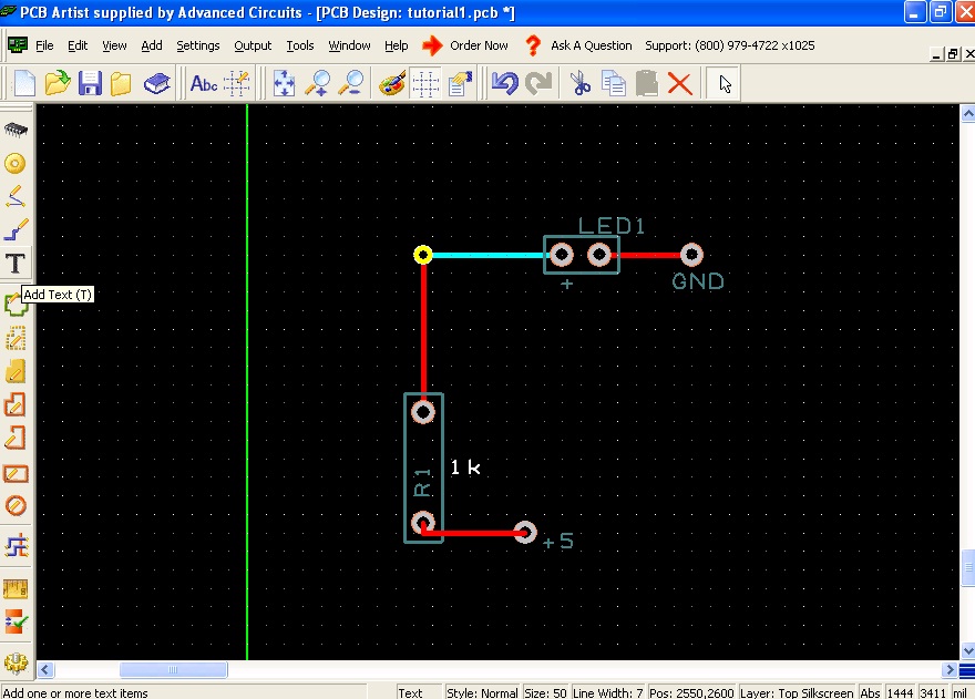
Add some text reminders to the silkscreen layer to remind yourself where to solder the power and ground, what direction the LED goes, and what resistor to use.
When your board is complete, use the Design Rule Check to automatically look for errors in connecting pins and accidentally crossed traces. You can check all the boxes.
Go to Settings, PCB Configuration to make your board bigger or smaller or change other properties. You can also click on specific edges of your board to resize the board, or use the arrow to drag a box around all the components to select them and drag them around inside the board.
Use this document, Student Order Process, to purchase a board with the $33 Student Discount. (Maximum board size for this special is 60 square inches.)
Go back to PCB Configuration and Enter Student in the Special Requirements section.
Go to Output, Submit Order. PCB Artist will perform a Design Rule Check. After that, enter the Promotion Code 33each. If you do not have an Advanced Circuits account, go to 4pcb.com and make one. Then you may order your board.
Adding a Component to the Library
A majority of the time the component you want to use is not in the existing libraries, therefore, you have to create a component. A component consists of a schematic symbol, a pcb symbol and a mapping between the pins of the schematic symbol and the pcb symbol. This section details how to create a component using the SN74HC04 Hex Inverter as an example.
Create a Schematic Symbol
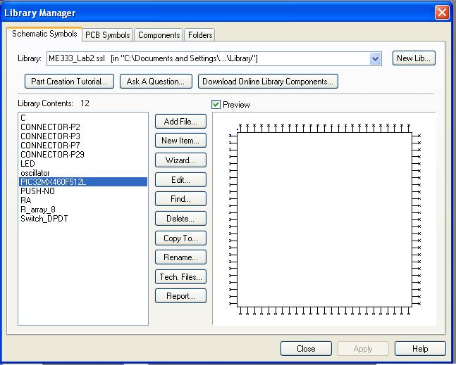
With PCBArtist open (it doesn't matter if any schematics or pcb files are open), click on the blue book at the top of the screen.

This opens the Library Manager of schematic symbols, pcb symbols and components. It will look something similar to the image below.
To make a component, we first need to download the datasheet of the component. Download the datasheet for the Hex Inverter here.
On the first page of the datasheet, we can find a schematic of the component for SN74HC04. We will use this schematic to make our schematic in PCB Artist.
- In PCBArtist, click on the 'Schematic Tab' of the Library Manager.
- Click on the 'Wizard' Button in the middle of the window to begin creating a schematic symbol.
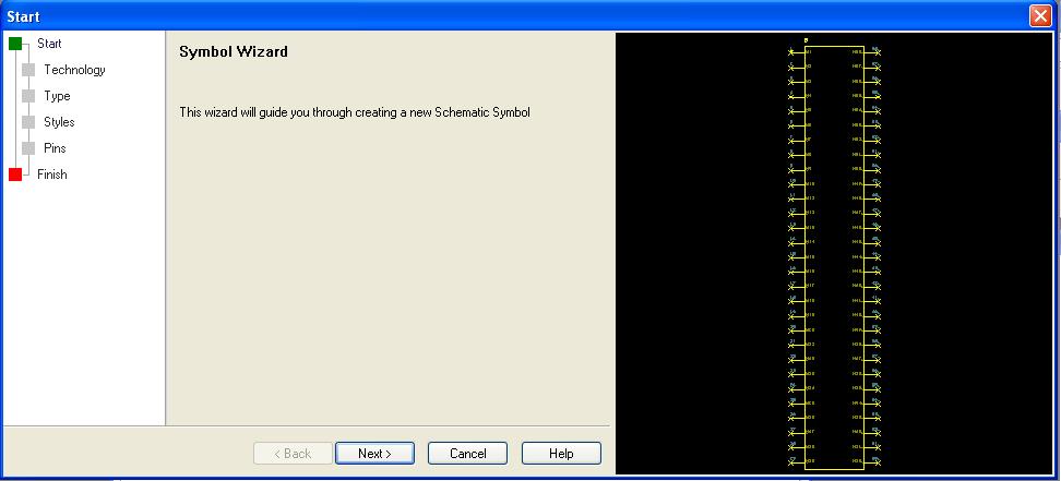
This wizard will help you make your schematic symbols.
- Click 'Next'
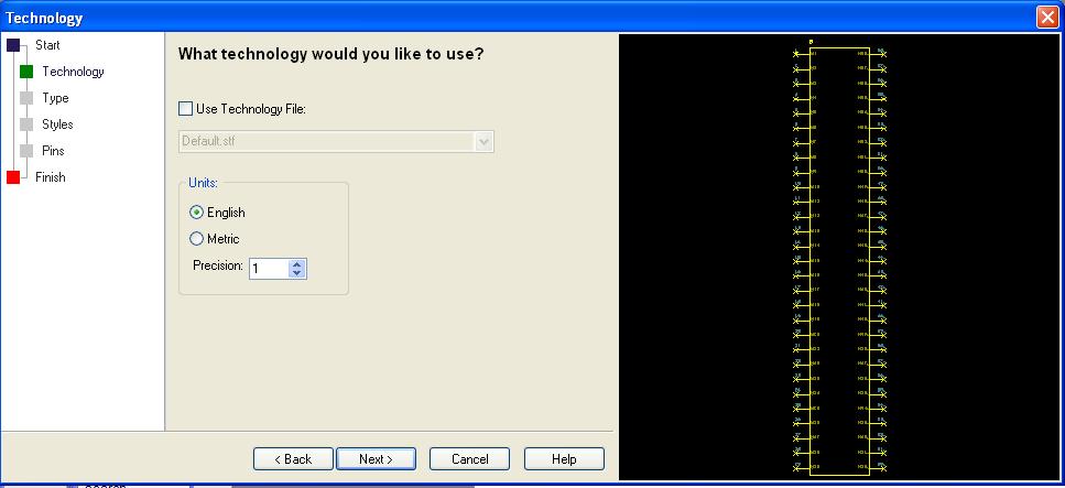
- Choose English with a precision of 1 (these are the units for the symbol)
- Click 'Next'
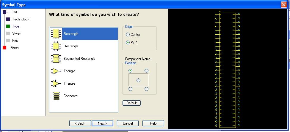
- Next we are going to choose the type of symbol. Our chip has pins on two sides so select the rectangle with pins on two sides (the first one).
- Select the 'center' option for Origin. If you decide to rotate the symbol, it will rotate about this point.
- Select the top left corner for Component Name. This indicates where the component name will be placed.
- Click 'Next'
- In the next window, you can choose how you want the pins to be represented, the size of these and the length of the lines going to the pins. Leave these with the default values.
- Click 'Next'
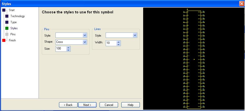
The next window determines the number of pins on each side of the component and some dimensions.
- Enter 7 for both Pins on left and Pins on Right.
- The other dimensions are not as important for the schematic, leave these as the default. (They can be editted later if too big or too small).
- The last part on this page describes how the pins are numbered. Since the schematic on the datasheet spirals the numbers, select the 'Spiral Round' option.
- Click 'Next'
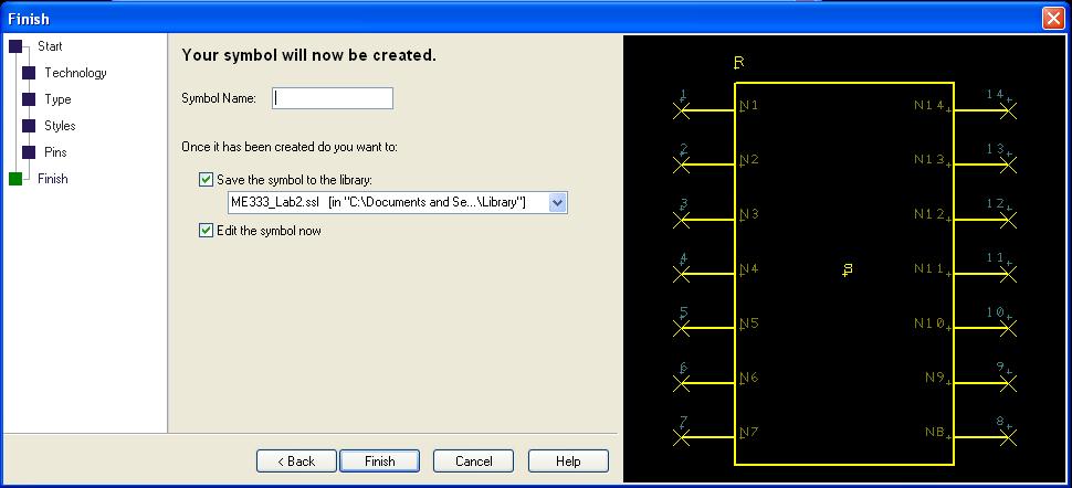
The last window is where you name the symbol and save it to a specific library.
- Name the component SN74HC04_Inverter and save it in the ME333_Lab2 Library that you downloaded above.
- Click Finish
You have now created a schematic symbol. If you checked the 'Edit the symbol now' box, you can see the schematic and edit if you want. We won't do any editting right now though.
Create a PCB Symbol
The next step is to create a pcb symbol for the component. This will be the footprint on your PCB. Look at the datasheet again and find the Plastic Dual-In Line Package footprint for the SN74HC04 (page 10). This tells us the dimensions we need for our footprint.
- Click on the Library Manager (blue book).
- Go to the PCB Symbols tab.
- Click on the Wizard again.
- Click Next on the start up window.
- On the Technology window, choose English with 'thou' as the unit and precision of 1. We choose this because it is the smallest unit on the datasheet for the English units.
The next window is the footprint type.
- Select DIP type (the top left).
- For Origin - select center
- For Name - select center - this is where the name will be displayed on the PCB
- Click 'Next'
The next window describes the pads on the PCB. This window will be different for the different types of chips.
- Choose 14 pads
- For the Pad Style, choose 'Round' and leave Style blank.
The units are in thousands of inches
- e = 100 for 0.1 in pitch (as shown on the datasheet).
- E = 400. We can put this value between 325 and 430 as shown on the datasheet, but we also know that the chip can plug into a breadboard (spacings of 0.1 in), so 400 thou is a good number.
- PW = 60 and HD = 30. HD refers to the hole diameter for the pin. The pin diameter is around 20 thou as shown on the datasheet, so 30 thou is a good number with extra space. PW is the pad width (extra copper) surrounding the hole. Extra 30 thou is generally a good pad width.
- Choose Pin 1 Position to be the lower left corner (same as in the footprint on the datasheet)
- We don't want the pin numbers to be displayed on the PCB so select Hide for the Pin Numbers
- Pin number is counter clockwise.
- Click Next
The next window describes the silk screen (the writing on top of the PCB).
- Click Yes
- Layer - Top Silkscreen
- Inside pads by 25 (sometimes you may want the silk screen to be outside the pads, but it is really your choice)
- Include Marks - Notch at end (12.5) --> this helps you figure out the orientation of the component
- Click Next
The next window asks if you want a placement shape (rectangle) around the entire component. We are not going to include this.
- Click No
- Click Next
- On the final window, name it SN74HC04_Inverter (same name as the schematic) and save it in the ME333 Library.
- Click Finish
You have now created a PCB footprint.
Create a Component
We created a schematic symbol and a pcb symbol above. Now we are going to create a component to link the two symbols.
- Click on the Library Manager and go to the Component tab.
- Click on the Wizard button
- Click Next on the opening window
The first window allows you to select what type of component you are making. You can make a Normal Component (both Schematic and PCB), only a Schematic component or only a PCB component.
- Select Normal Component
- Click Next
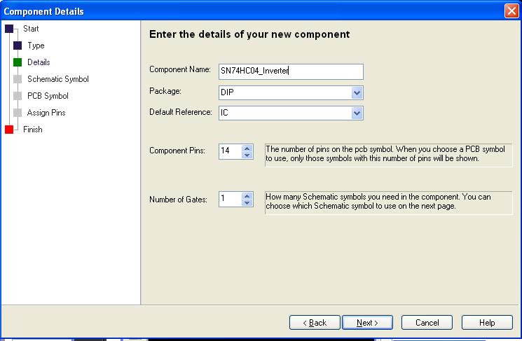
This windows contains the details for the component.
- Name = SN74HC04_Inverter (same as the symbols)
- Package - type DIP (this really doesn't matter)
- Default Reference - choose IC for integrated circuit
- Component pins - 14
- Number of Gates - 1 - this is the number of times your schematic symbol is needed for the component
- Click Next
In the next window you select the schematic symbol that you want to use
- Select SN74HC04_Inverter from the ME333 Library
- Click Next
In the PCB window, you select the pcb symbol that you want to use
- Select SN74HC04_Inverter from the ME333 Library
- Click Next
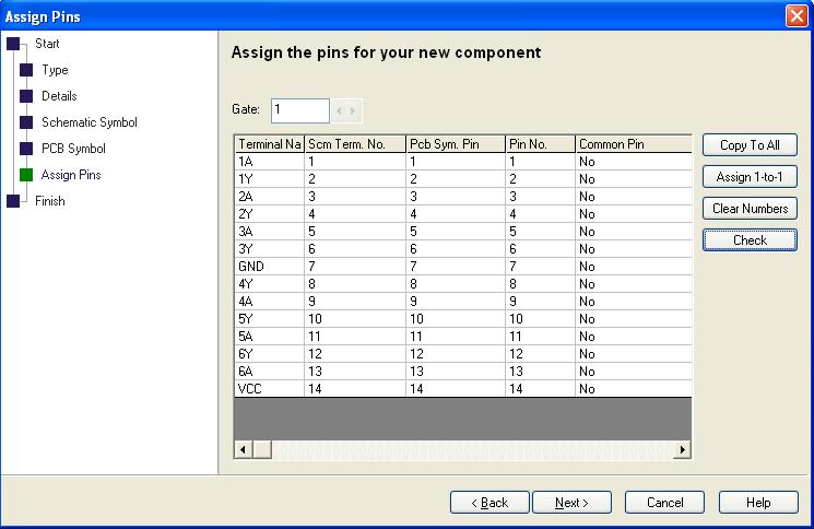
The next window assigns the pins from the schematic to the pcb. Since we choose our pins in the schematic and pcb to have the same order:
- Select Assign 1-to-1 button to assign Pin 1 Schematic to Pin 1 PCB ... etc
We can also choose to add names to each pin.
- Assign the pins names (1A,1Y,GND..etc) to each of the pins as shown on the datasheet.
- Click Next
On the final window:
- Click Save the component to the library --> Put it in the ME333 library
If you want to edit the component now (check the next box)
- Click finish
You have now created a component and can use it with schematics and pcbs.
Practice Making a PCB
After reviewing this tutorial, you are ready to Practice Making a PCB.
