Difference between revisions of "Diodes and Transistors"
| (93 intermediate revisions by 4 users not shown) | |||
| Line 1: | Line 1: | ||
==Diodes== |
==Diodes== |
||
Symbol for |
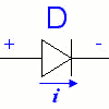
Symbol for a diode: [[Image:diode_symbol.gif]] |
||
We can take advantage of the properties of a p-n junction to make a '''diode''', which is an electrical component that only allows current flow in one direction. |
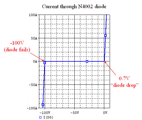
We can take advantage of the properties of a p-n junction to make a '''diode''', which is an electrical component that only allows current flow in one direction. A diode made of silicon needs about 0.7V across it in the forward direction ('''forward biased''') in order to conduct. At a large negative voltage ('''reverse biased'''), the diode fails and the current forces its way though. This is known as '''diode breakdown'''. |
||
[[Image:diode_N4002_profile.gif]] |
[[Image:diode_N4002_profile.gif]] |
||
| Line 8: | Line 8: | ||
===Applications of Diodes=== |
===Applications of Diodes=== |
||
====Half-Wave Rectifier==== |
====Half-Wave Rectifier==== |
||
A half-wave rectifier |
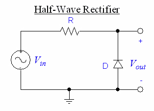
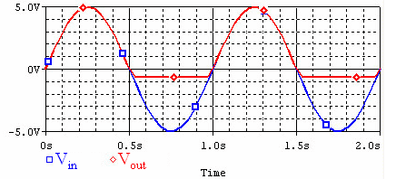
A half-wave rectifier cuts off half of a sine wave, leaving only the positive or negative side (although not perfectly, because of the diode voltage drop). |
||
The schematic for a simple rectifier: |
The schematic for a simple rectifier: |
||
| Line 19: | Line 19: | ||
====Flyback Diode==== |
====Flyback Diode==== |
||
An approximate model of a DC motor is a resistor and inductor in series. |
An approximate model of a DC motor is a resistor and inductor in series. (For more details on DC motors, see the section on [[Brushed_DC_Motor_Theory|brushed DC motors]].) If there is a current <math>i</math> through the motor, and we suddenly break the circuit by opening a switch, for instance, there will be a spike in the voltage across the inductor. This is because the current has to instantly go to zero (there is no longer a path for it), and the voltage across the inductor is proportional to the rate of change of current, |
||
<math>v_L = L (di/dt)</math>. This may exhibit itself in a spark at the switch. A mechanical analog of instantly zeroing the current through an inductor is bringing the velocity of a moving mass to zero, instantly. |
|||
To alleviate this problem, we can put a '''flyback diode''' across the motor terminals, as shown below: |
|||
[[Image:diode_flyback_schematic.gif]] |
[[Image:diode_flyback_schematic.gif]] |
||
This |
This diode allows current to continue flowing through the motor, satisfying the inductor's "desire" to continue to allow current to flow. The energy in the inductor is dissipated over time by the resistance of the motor, and the current drops smoothly to zero. Note that no current flows through the diode when the switch is closed, as it is reverse biased. |
||
The flyback diode must be sufficiently large to carry the potentially large currents of the motor. |
|||
'''Question''': If the voltage supply is +10V relative to ground and the diode drop is 0.7V, what is the voltage across the inductor immediately after the switch is opened? Make sure you have the sign right, where positive voltage means the left side has a higher potential than the right side. (Remember, the voltage across an inductor can change discontinuously, but not the current, if there is any possible path for the current.) |
|||
====Peak Detector==== |
====Peak Detector==== |
||
| Line 36: | Line 43: | ||
Each time the input voltage dips, the diode prevents the capacitor from draining. |
Each time the input voltage dips, the diode prevents the capacitor from draining. |
||
There are two problems with this circuit: First, the voltage |
There are two problems with this circuit: First, the voltage at <math>V_{out}</math> is always one diode drop less than the maximum <math>V_{in}</math>. Second, the circuit has a very low impedance, and the capacitor drains a lot of current. A better peak detector can be built with op-amps. |
||
====Voltage Clamp==== |
====Voltage Clamp==== |
||
A voltage clamp |
A voltage clamp limits the output voltage, which is useful when we need to protect circuits from high voltages. We specify the maximum and minimum voltage we want by applying voltages across a diode. We must also take into account the voltage drop, so the voltages we apply should be <math>V_{max}-0.7</math> and <math>V_{min}+0.7</math> |
||
[[Image:diode_voltage_clamp.gif]] |
[[Image:diode_voltage_clamp.gif]] |
||
In this |
In this circuit, if <math>V_{in}</math> exceeds <math>V_{max}</math>, diode <math>D_1</math> becomes forward biased and conducts, thus forcing <math>V_{out}</math> to stay at <math>V_{max}</math>. If <math>V_{in}</math> drops lower than <math>V_{min}</math>, diode <math>D_2</math> conducts and prevents the <math>V_{out}</math> from dropping any lower. |
||
==Zener Diodes== |
==Zener Diodes== |
||
| Line 57: | Line 64: | ||
[[Image:zener_voltage_regulator.gif]] |
[[Image:zener_voltage_regulator.gif]] |
||
<math> |
<math>V_{out}</math> is the '''reverse breakdown voltage''' or '''zener voltage'''. In the circuit, ''V'' is greater than ''V<sub>Z</sub>''. This voltage regulator can only step down the voltage, not up. |
||
Even if the current through the diode fluctuates, the voltage |
Even if the current through the diode fluctuates, the voltage remains fairly stable. Choose a resistance R large enough such that the power specs of the zener diode are not exceeded, but not so large that it limits our current too much. |
||
For example, if our diode has a zener voltage of 5V and can handle 1W, and our voltage source has a maximum voltage of 20V: |
For example, if our diode has a zener voltage of 5V and can handle 1W, and our voltage source has a maximum voltage of 20V: |
||
The largest amount of current our diode |
The largest amount of current our diode ever has to handle is the current through the diode when there is no external load. Therefore: |
||
<math>I_{z(max)}=\frac{(20-5)V}{R}</math> |
<math>I_{z(max)}=\frac{(20-5)V}{R}</math> |
||
| Line 78: | Line 85: | ||
symbol for an LED: [[Image:LED_symbol.gif]] |
symbol for an LED: [[Image:LED_symbol.gif]] |
||
An LED is a type of diode that emits visible or infrared light proportional to the current passing through it (up to a maximum before it burns out). |
|||
A typical LED shines its brightest between 5mA and 30mA. Beyond its rated current, it may burn out. |
|||
[[Image:LED_photo.jpg|thumb|right|A photograph of an LED]] |
|||
Notice that on the LED pictured at the right, one of the legs is longer. The longer leg is the positive terminal. However, do not rely on the length of the leg to determine the polarity, because you will probably snip the legs short later on. Instead, look at the side of the plastic lens, and notice that it's not perfectly round; one side is flattened. The flattened side is the ground. |
|||
[[Image:LED_inside_photo.jpg]] |
|||
<br clear="all"> |
|||
==Photodiode== |
|||
Symbol for a photodiode:[[Image:photodiode_symbol.gif]] |
|||
Go to the [[Photodiodes_and_Phototransistors#Photodiodes|photodiode]] page for information on photodiodes. |
|||
==Bipolar Junction Transistors (BJT)== |
==Bipolar Junction Transistors (BJT)== |
||
| Line 105: | Line 129: | ||
BJTs have three regions of operation: |
BJTs have three regions of operation: |
||
Cutoff: <math>I_C=0</math> (no collector current) |
Cutoff (<math>V_{BE} < 0.7V</math>): <math>I_C=0</math> (no collector current) |
||
Active: <math>I_C=</math>''β''<math>I_B</math> (collector current is proportional to base current by factor ''β'') |
Active (<math>V_{BE}</math> ≈ <math>0.7V</math>): <math>I_C=</math>''β''<math>I_B</math> (collector current is proportional to base current by factor ''β'', which is typically about 100) |
||
Saturated: <math>V_{CE}</math> ≈ <math>0.2V</math> (for npn); |
Saturated (<math>V_{BE}</math> ≈ <math>0.7V</math>): <math>V_{CE}</math> ≈ <math>0.2V</math> (for npn); collector current is mainly limited by its subsequent circuitry. |
||
===Applications of BJTs=== |
===Applications of BJTs=== |
||
====Common Emitter Amplifier Circuit==== |
====Common Emitter Amplifier Circuit==== |
||
In a common emitter circuit, the emitter of a transistor is grounded and an input voltage is applied at the base. An example common emitter circuit with a transistor (''β''=100) is drawn below: |
In a common emitter circuit, the emitter of a transistor is grounded and an input voltage is applied to the resistor at the base. An example common emitter circuit with a transistor (''β''=100) is drawn below: |
||
[[Image:transistor_common_emitter.gif]] |
[[Image:transistor_common_emitter.gif]] |
||
If <math>V_{in}</math> < 0.7V (same as the diode drop), the p-n junction is not forward biased |
If <math>V_{in}</math> < 0.7V (same as the diode drop), the p-n junction is not forward biased, there is no base current, and <math>I_C</math> is equal to 0. |
||
If <math>V_{in}</math> > 0.7V, then |
If <math>V_{in}</math> > 0.7V, then |
||
<math>I_B=(V_{in}-V_B)/10000=(V_{in}-0.7)/10000</math> |
<math>I_B=(V_{in}-V_B)/10000</math>''Ω''<math>=(V_{in}-0.7)/10000</math>''Ω'' |
||
<math>I_C=</math>''β''<math>(V_{in}-0.7)/10000</math> |
<math>I_C=</math>''β''<math>(V_{in}-0.7)/10000</math>''Ω'' |
||
Now we |
Now we calculate how large <math>V_{in}</math> has to be to saturate the transistor. When <math>V_{CE}=0.2V</math>, the transistor becomes saturated. If the drop across the collector and emitter of the transistor is equal to 0.2V, then the drop across the resistor at the collector must equal 9.8V. Thus: |
||
<math>I_C=9.8/1000=9.8mA</math> |
<math>I_C=9.8/1000</math>''Ω''<math>=9.8mA</math> |
||
<math>I_B=I_C/</math>''β''<math>=0.098mA</math> |
<math>I_B=I_C/</math>''β''<math>=0.098mA</math> |
||
| Line 146: | Line 170: | ||
====Emitter Follower==== |
====Emitter Follower==== |
||
The emitter follower is a very simple current amplifier, taking advantage of the fact that <math>I_C=</math>''β''<math>I_B</math>. The high input impedance means that our imput signal does not need to work as hard. |
The emitter follower is a very simple current amplifier, taking advantage of the fact that <math>I_C=</math>''β''<math>I_B</math>. The high input impedance means that our imput signal does not need to "work" as hard. |
||
[[Image:transistor_emitter_follower.gif]] |
[[Image:transistor_emitter_follower.gif]] |
||
| Line 159: | Line 183: | ||
If <math>V_{in}</math> > 0.7V, then the current is amplified by the npn transistor. |
If <math>V_{in}</math> > 0.7V, then the current is amplified by the npn transistor. |
||
If <math>V_{in}</math> < 0.7V, then the current is amplified by the pnp transistor. |
If <math>V_{in}</math> < -0.7V, then the current is amplified by the pnp transistor. |
||
Beware that there is a “dead band” when V<sub>in</sub> is between 0.7V and -0.7V, because the voltage has not pass the cutoff voltage for either transistor. This is known as '''crossover distortion'''. |
|||
=====Push-Pull Follower Example: A (Poor) Motor Speed Controller===== |
|||
=====Motor Speed Controller Example (Lab 1)===== |
|||
Suppose we want to control the speed of a motor by varying the input voltage between +5V and -5V. We attempt to do this by setting put a voltage divider with a potentiometer like in the circuit below. |
Suppose we want to control the speed of a motor by varying the input voltage between +5V and -5V. We attempt to do this by setting put a voltage divider with a potentiometer like in the circuit below. |
||
[[Image:speed_controller_simple.gif]] |
|||
[[Image:speed_controller_simple.gif]]We model our motor with a simple resistor RL. If ''RL'' is infinitely large (no current flowing through), then there will be a 7.2V drop across ''R1'' and ''R'', and <math>V_{in}</math> can take a value between 4.8V and -4.8V. |
|||
We model our motor with a simple resistor <math>R_L</math>. If <math>R_L</math> is infinitely large (no current flowing through), then there will be a 7.2V drop across <math>R_1</math> and <math>R_3</math>, and <math>V_{in}</math> can take a value between 4.8V and -4.8V. |
|||
For the maximum voltage case, our circuit with voltage sources looks like this: |
|||
For the maximum voltage case (we turn the POT all the way to one side), our circuit with voltage sources looks like this: |
|||
[[Image:speed_controller_sources.gif]] We know that RL is ''not'' infinitely large because motors can draw quite a lot of current. If ''RL=0'' (short ciruict), then the <math>V_{in}=0</math>. We can expect <math>V_{in}</math> to be somewhere between 0V and 4.8V. |
|||
[[Image:speed_controller_sources.gif]] |
|||
We know that <math>R_L</math> is ''not'' infinitely large because motors can draw quite a lot of current. If <math>R_L=0</math> (short circuit), then the <math>V_{in}=0V</math>. We can expect <math>V_{in}</math> to be somewhere between 0V and 4.8V. |
|||
We can solve the circuit with the following equations: |
We can solve the circuit with the following equations: |
||
| Line 183: | Line 214: | ||
<math>V_{in}=I_2R_L</math> |
<math>V_{in}=I_2R_L</math> |
||
Solving the equations yields: |
|||
<math>V_{in}=24R_L/(2625+5R_L)</math> |
|||
If <math>R_L=10</math>Ω, we can plug it in and find that <math>V_{in}</math> is only equal to 0.0897V and the current is equal to 8.97mA—not nearly enough to drive the motor. |
|||
It turns out that the voltage controlling circuit cannot supply much current, so the low impedance of the motor drains what current is available very quickly and pulls down the output voltage. When the impedance of the power source is much larger than the impedance of the load, this is known as '''loading'''. |
|||
We can't use this circuit to drive a motor directly, because our controller needs to see a high impedance, but our motor has a low impedance—we need a way to isolate the controller from the motor. This is where we can use our push-pull current amplifier. We connect it to our circuit as shown below to better isolate the controller from the motor and amplify the current. Unfortunately, the transistors only have a gain of about 100, so the controller circuit still does not see an infinite impedance. |
|||
[[Image:speed_controller_push_pull.gif]] |
|||
====Emitter Follower Voltage Regulator==== |
|||
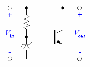
With our previous voltage regulator with the zener diode, we had the problems of the zener diode wasting power and needing a high power diode if there was a lot of current going through the diode. If we add an emitter-follower, we can use a much smaller diode and less current to achieve the same effect. |
|||
[[Image:emitter_follower_voltage_regulator.gif]] |
|||
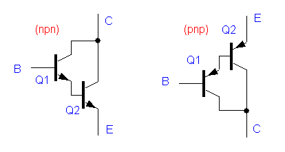
====Darlington Pair==== |
|||
If we need a very high current gain, we replace a transistor with a ''Darlington pair''. The current gain is now: |
|||
<math>\beta=\beta_1\beta_2</math> |
|||
[[Image:Darlington_pairs.gif]] |
|||
==Field Effect Transistors (FET)== |
|||
FETs are a type of transistor that uses a voltage input to control its conductivity (as opposed to using the current like a BJT). The input impedance is very high and thus draws very little current. There are three general types of FETs: |
|||
1.enhancement mode metal-oxide-semiconductor FETs (MOSFETs) |
|||
2.depletion mode MOSFETs |
|||
3.Junction FETs (JFETs) |
|||
===MOSFETs=== |
|||
The symbol for a MOSFET looks like this: [[Image:mosfet_with_b_symbol.gif]] |
|||
where G is for '''gate''', S for '''source''', D for '''drain''', and B for '''substrate'''. |
|||
However, since B is usually connected to S, the symbol is often simply drawn as: [[Image:mosfet_without_b_symbol.gif]] |
|||
Electrons flow from the source to the drain, so the current flows from drain to source. The gate receives the input voltage. The gate pin is offset towards to source pin to help is differentiate between the source and drain pins. |
|||
MOSFETS come in '''enhancement''' and '''depletion''' modes. An enhancement mode MOSFET allows a current to flow only if a positive voltage is applied, while depletion mode MOSFETs allows a current to flow even if no voltage difference is applied. Increasing the voltage increases the current, and it takes a ''negative'' voltage to turn off a depletion mode MOSFET. MOSFETS, like BJTs, also come in ''p'' and ''n'' types. The different MOSFETS and their corresponding symbols are below: |
|||
{| border="1" cellspacing="0" cellpadding="5" align="center" |
|||
|+'''MOSFETS''' |
|||
|- |
|||
! !!n-channel!! p-channel |
|||
|- |
|||
!Enhancement!! [[Image:MOSFET_n_enhance.gif]] || [[Image:MOSFET_p_enhance.gif]] |
|||
|- |
|||
!Depletion!! [[Image:MOSFET_n_deplete.gif]] || [[Image:MOSFET_p_deplete.gif]] |
|||
|- |
|||
|} |
|||
===JFETs=== |
|||
JFETs are very similar to MOSFETS, but they only come in the depletion-mode variety. JFET consume little power, so they are often found in low-power applications. The symbols for JFETs are below: |
|||
{| border="1" cellspacing="0" cellpadding="5" align="center" |
|||
|+'''MOSFETS''' |
|||
|- |
|||
! !!n-channel!! p-channel |
|||
|- |
|||
! Depletion!! [[Image:JFET_n.gif]] || [[Image:JFET_p.gif]] |
|||
|- |
|||
|} |
|||
==Phototransistor== |
|||
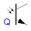
Symbol for a phototransistor:[[Image:photo_transistor_symbol.gif]] |
|||
Notice that the phototransistor only has two legs. |
|||
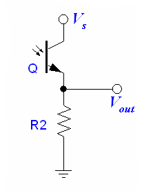
The collector current of a phototransistor is proportional to the light or infrared light received. |
|||
[[Image:photo_transistor_diagram.gif]] |
|||
<math>V_{out}</math> can take a value between ''0V'' and <math>V_s-0.2V</math>. |
|||
Go to the [[Photodiodes_and_Phototransistors#Phototransistors|phototransistor]] page for more information on phototransistors. |
|||
Emitter/Detector pair: |
|||
[[Image:emitter_detector_pair.gif]] |
|||
An emitter-detector pair is a very useful circuit that can be used to isolate two circuits or used as a sensor. Among other applications, it can be used to detect changes in the distance between the emitter and detector (changing the distance changes the intensity of the received light) or used to detect interruptions in the light beam. |
|||
A [[Photodiodes_and_Phototransistors#Photodiodes|photodiode]] can also be used instead of a phototransistor in many applications; a photodiode cannot supply as much current, but has a faster response time. |
|||
==References== |
|||
Alciatore, David G. and Michael B. Histand. <u>Introduction to Mechatronics and Measurement Systems</u>. 2nd ed. New York, NY:McGraw-Hill, 2003. |
|||
Latest revision as of 20:30, 11 January 2010
Diodes
We can take advantage of the properties of a p-n junction to make a diode, which is an electrical component that only allows current flow in one direction. A diode made of silicon needs about 0.7V across it in the forward direction (forward biased) in order to conduct. At a large negative voltage (reverse biased), the diode fails and the current forces its way though. This is known as diode breakdown.
Applications of Diodes
Half-Wave Rectifier
A half-wave rectifier cuts off half of a sine wave, leaving only the positive or negative side (although not perfectly, because of the diode voltage drop).
The schematic for a simple rectifier:
The graph for half-wave rectifier:
Flyback Diode
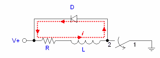
An approximate model of a DC motor is a resistor and inductor in series. (For more details on DC motors, see the section on brushed DC motors.) If there is a current through the motor, and we suddenly break the circuit by opening a switch, for instance, there will be a spike in the voltage across the inductor. This is because the current has to instantly go to zero (there is no longer a path for it), and the voltage across the inductor is proportional to the rate of change of current, . This may exhibit itself in a spark at the switch. A mechanical analog of instantly zeroing the current through an inductor is bringing the velocity of a moving mass to zero, instantly.
To alleviate this problem, we can put a flyback diode across the motor terminals, as shown below:
This diode allows current to continue flowing through the motor, satisfying the inductor's "desire" to continue to allow current to flow. The energy in the inductor is dissipated over time by the resistance of the motor, and the current drops smoothly to zero. Note that no current flows through the diode when the switch is closed, as it is reverse biased.
The flyback diode must be sufficiently large to carry the potentially large currents of the motor.
Question: If the voltage supply is +10V relative to ground and the diode drop is 0.7V, what is the voltage across the inductor immediately after the switch is opened? Make sure you have the sign right, where positive voltage means the left side has a higher potential than the right side. (Remember, the voltage across an inductor can change discontinuously, but not the current, if there is any possible path for the current.)
Peak Detector
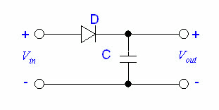
We can make a peak detector if we hook up our circuit like this:
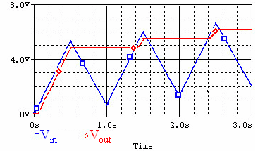
The graph of the input and output voltages looks like this:
Each time the input voltage dips, the diode prevents the capacitor from draining.
There are two problems with this circuit: First, the voltage at is always one diode drop less than the maximum . Second, the circuit has a very low impedance, and the capacitor drains a lot of current. A better peak detector can be built with op-amps.
Voltage Clamp
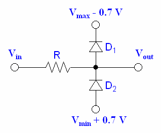
A voltage clamp limits the output voltage, which is useful when we need to protect circuits from high voltages. We specify the maximum and minimum voltage we want by applying voltages across a diode. We must also take into account the voltage drop, so the voltages we apply should be and
In this circuit, if exceeds , diode becomes forward biased and conducts, thus forcing to stay at . If drops lower than , diode conducts and prevents the from dropping any lower.
Zener Diodes
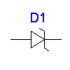
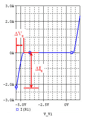
Zener diodes have a low breakdown voltage, or zener voltage, and can allow reverse current to flow without being destroyed. A good zener diode can also maintain a fairly constant voltage over a large range of currents. The voltage-current graph of a zener diode looks like this:
Voltage Regulator
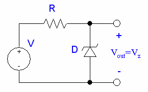
We can use a zener diode to build a voltage regulator like this:
is the reverse breakdown voltage or zener voltage. In the circuit, V is greater than VZ. This voltage regulator can only step down the voltage, not up.
Even if the current through the diode fluctuates, the voltage remains fairly stable. Choose a resistance R large enough such that the power specs of the zener diode are not exceeded, but not so large that it limits our current too much.
For example, if our diode has a zener voltage of 5V and can handle 1W, and our voltage source has a maximum voltage of 20V:
The largest amount of current our diode ever has to handle is the current through the diode when there is no external load. Therefore:
This means that we need at least 75Ω to protect our diode. Keep in mind that we must meet the power ratings for our resistor as well.
Because current is flowing through the resistor and diode even when there is no load, power is being wasted. We can do better with voltage regulator chips like a 7805 chip (78xx for xx volts).
LEDs (Light Emitting Diode)
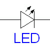
An LED is a type of diode that emits visible or infrared light proportional to the current passing through it (up to a maximum before it burns out).
A typical LED shines its brightest between 5mA and 30mA. Beyond its rated current, it may burn out.
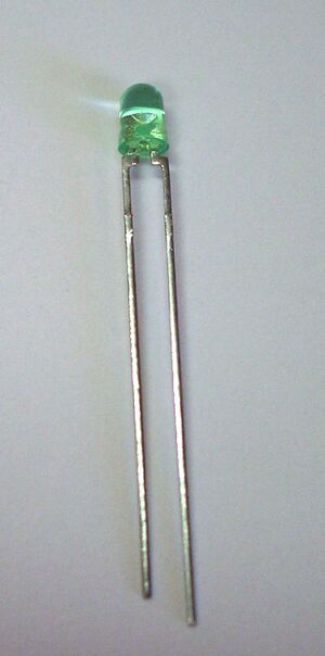
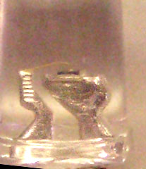
Notice that on the LED pictured at the right, one of the legs is longer. The longer leg is the positive terminal. However, do not rely on the length of the leg to determine the polarity, because you will probably snip the legs short later on. Instead, look at the side of the plastic lens, and notice that it's not perfectly round; one side is flattened. The flattened side is the ground.
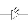
Photodiode
Go to the photodiode page for information on photodiodes.
Bipolar Junction Transistors (BJT)
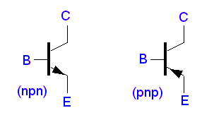
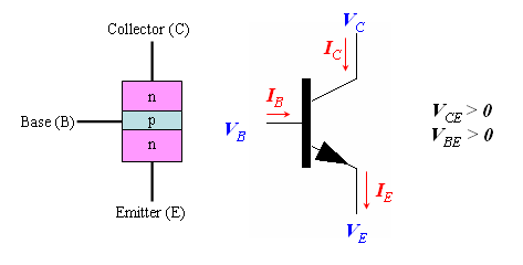
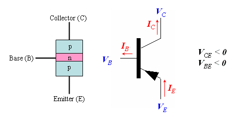
There are two types of of BJTs; n-p-n and p-n-p:
npn
pnp
For the transistors, we have the following relationship for the voltages and curents:
Under normal operation, BE is forward biased, and CB is reverse biased.
BJTs have three regions of operation:
Cutoff (): (no collector current)
Active ( ≈ ): β (collector current is proportional to base current by factor β, which is typically about 100)
Saturated ( ≈ ): ≈ (for npn); collector current is mainly limited by its subsequent circuitry.
Applications of BJTs
Common Emitter Amplifier Circuit
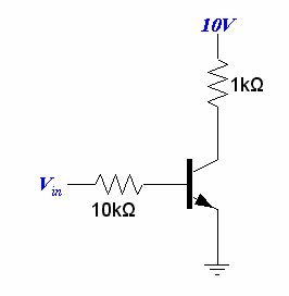
In a common emitter circuit, the emitter of a transistor is grounded and an input voltage is applied to the resistor at the base. An example common emitter circuit with a transistor (β=100) is drawn below:
If < 0.7V (same as the diode drop), the p-n junction is not forward biased, there is no base current, and is equal to 0.
If > 0.7V, then
ΩΩ
βΩ
Now we calculate how large has to be to saturate the transistor. When , the transistor becomes saturated. If the drop across the collector and emitter of the transistor is equal to 0.2V, then the drop across the resistor at the collector must equal 9.8V. Thus:
Ω
β
Then we find :
Ω
or greater.
cutoff: < 0.7V
active:0.7V < <1.68V
saturated:1.68V <
If we are using the transistor as a switch, we should fully saturate it to save power and reduce heat.
Emitter Follower
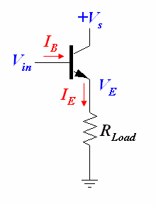
The emitter follower is a very simple current amplifier, taking advantage of the fact that β. The high input impedance means that our imput signal does not need to "work" as hard.
Push-Pull Follower
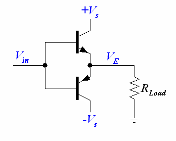
If we put two emitter followers together (npn transistor for positive voltages; pnp transistor for negative voltages), we get a push-pull follower.
If > 0.7V, then the current is amplified by the npn transistor.
If < -0.7V, then the current is amplified by the pnp transistor.
Beware that there is a “dead band” when Vin is between 0.7V and -0.7V, because the voltage has not pass the cutoff voltage for either transistor. This is known as crossover distortion.
Push-Pull Follower Example: A (Poor) Motor Speed Controller
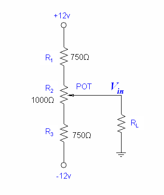
Suppose we want to control the speed of a motor by varying the input voltage between +5V and -5V. We attempt to do this by setting put a voltage divider with a potentiometer like in the circuit below.
We model our motor with a simple resistor . If is infinitely large (no current flowing through), then there will be a 7.2V drop across and , and can take a value between 4.8V and -4.8V.
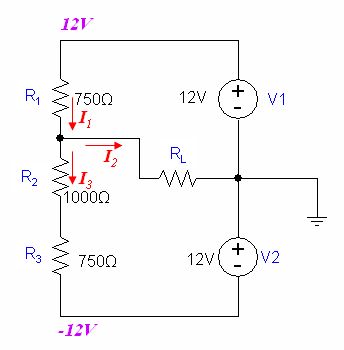
For the maximum voltage case (we turn the POT all the way to one side), our circuit with voltage sources looks like this:
We know that is not infinitely large because motors can draw quite a lot of current. If (short circuit), then the . We can expect to be somewhere between 0V and 4.8V.
We can solve the circuit with the following equations:
KCL:
KVL:
Solving the equations yields:
If Ω, we can plug it in and find that is only equal to 0.0897V and the current is equal to 8.97mA—not nearly enough to drive the motor.
It turns out that the voltage controlling circuit cannot supply much current, so the low impedance of the motor drains what current is available very quickly and pulls down the output voltage. When the impedance of the power source is much larger than the impedance of the load, this is known as loading.
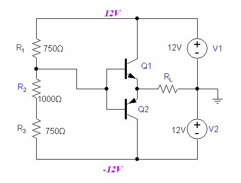
We can't use this circuit to drive a motor directly, because our controller needs to see a high impedance, but our motor has a low impedance—we need a way to isolate the controller from the motor. This is where we can use our push-pull current amplifier. We connect it to our circuit as shown below to better isolate the controller from the motor and amplify the current. Unfortunately, the transistors only have a gain of about 100, so the controller circuit still does not see an infinite impedance.
Emitter Follower Voltage Regulator
With our previous voltage regulator with the zener diode, we had the problems of the zener diode wasting power and needing a high power diode if there was a lot of current going through the diode. If we add an emitter-follower, we can use a much smaller diode and less current to achieve the same effect.
Darlington Pair
If we need a very high current gain, we replace a transistor with a Darlington pair. The current gain is now:
Field Effect Transistors (FET)
FETs are a type of transistor that uses a voltage input to control its conductivity (as opposed to using the current like a BJT). The input impedance is very high and thus draws very little current. There are three general types of FETs:
1.enhancement mode metal-oxide-semiconductor FETs (MOSFETs)
2.depletion mode MOSFETs
3.Junction FETs (JFETs)
MOSFETs
The symbol for a MOSFET looks like this: 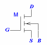
where G is for gate, S for source, D for drain, and B for substrate.
However, since B is usually connected to S, the symbol is often simply drawn as: 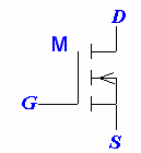
Electrons flow from the source to the drain, so the current flows from drain to source. The gate receives the input voltage. The gate pin is offset towards to source pin to help is differentiate between the source and drain pins.
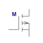
MOSFETS come in enhancement and depletion modes. An enhancement mode MOSFET allows a current to flow only if a positive voltage is applied, while depletion mode MOSFETs allows a current to flow even if no voltage difference is applied. Increasing the voltage increases the current, and it takes a negative voltage to turn off a depletion mode MOSFET. MOSFETS, like BJTs, also come in p and n types. The different MOSFETS and their corresponding symbols are below:
| n-channel | p-channel | |
|---|---|---|
| Enhancement | 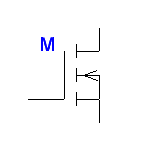 |
|
| Depletion | 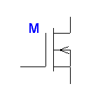 |
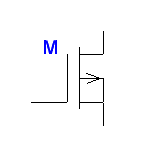
|
JFETs
JFETs are very similar to MOSFETS, but they only come in the depletion-mode variety. JFET consume little power, so they are often found in low-power applications. The symbols for JFETs are below:
| n-channel | p-channel | |
|---|---|---|
| Depletion | 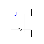 |
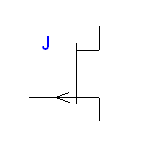
|
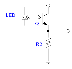
Phototransistor
Notice that the phototransistor only has two legs.
The collector current of a phototransistor is proportional to the light or infrared light received.
can take a value between 0V and .
Go to the phototransistor page for more information on phototransistors.
Emitter/Detector pair:
An emitter-detector pair is a very useful circuit that can be used to isolate two circuits or used as a sensor. Among other applications, it can be used to detect changes in the distance between the emitter and detector (changing the distance changes the intensity of the received light) or used to detect interruptions in the light beam.
A photodiode can also be used instead of a phototransistor in many applications; a photodiode cannot supply as much current, but has a faster response time.
References
Alciatore, David G. and Michael B. Histand. Introduction to Mechatronics and Measurement Systems. 2nd ed. New York, NY:McGraw-Hill, 2003.
