Semiconductors
Conductors and Insulators
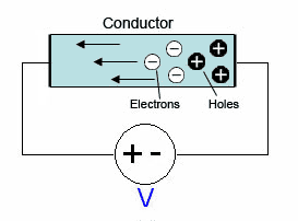
Conductors are able to accommodate an electron flow through them because the electrons in the atoms are not tightly bound to their atoms. When an electron leaves its atom, it leaves behind hole, which because of the absence of the electron, is positively charged since the atom started out neutral. This hole can be modeled as a positive charge. As electrons move towards one end of the conductor, they will leave holes at the opposite end, thus creating a "flow" of holes in the direction opposite the electron flow.
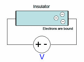
The electrons in insulators are tightly bound to their atoms, so they cannot flow.
Semiconductors
Semiconductors, such as silicon, are somewhere in between a conductor and an insulator. Some electrons in the semi-conductor are allowed to flow, especially when released by heat or light. Semiconductors allow us to build non-linear devices, such as computers.
We can increase the conductivity of semiconductors by doping, or interspersing atoms with more valence electrons into the lattice structure.
For example, we can dope silicon (which as four valence electrons) with arsenic (which has 5 valence electrons). The extra electron in the arsenic atom cannot form a covalent bond with the neighboring atoms, and thus is loosely bound and available as a charge carrier. This creates an n-type semiconductor, which has negative charge carriers.
We can also dope the silicon with boron or gallium, which have 3 valence electrons. The lack of an electron to complete all four covalent bonds in the lattice structure leaves a hole that can accept an electron. This creates a p-type semiconductor, which has positive charge carriers.
p-n junctions
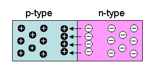
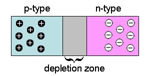
When we sandwich a p-type semiconductor with an n-type semiconductor, the electrons at the interface will jump into the holes, creating a depletion zone—an insulating section of semiconductor devoid of either type of charge carrier.
The electrons will jump into the holes across the border:
and will form the depletion zone:
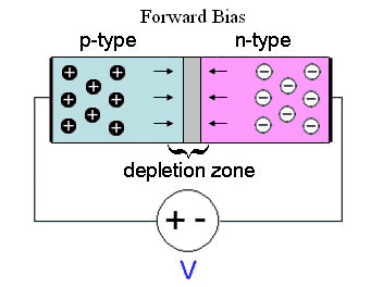
If we put a voltage across the semiconductors with the positive voltage on the p-type semiconductor, we will create a forward bias. The positive voltage will repel the holes, and the negative voltage will repel the electrons, pushing both towards the junction. This movement shrinks the depletion zone, and if our voltage is high enough, the depletion zone will become so thin that electrons will be able to tunnel through it. When this happens, current will be able to flow through the semi-conductors.
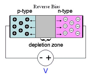
On the other hand, if we connect the positive voltage to the n-type semiconductor and the negative voltage to the p-type semiconductor, we will create a reverse bias. The negative voltage will attract the holes, and the positive voltage will attract the electrons. This will pull both holes and electrons away from the junction and widen the depletion zone. Because of this, no current can flow through the semiconductors. (However, if the voltage is high enough, current can still force its way across.)
