Example Writeup: Analog Input
Original Assignment
The goal of this assignment is to provide sample code and circuits that clearly demonstrate how to use the analog input capabilities of the PIC 18F4520 by giving a few examples.
Overview
You can assign from one to thirteen pins to be used as analog inputs. These pins are named AN0 through AN12. The set that you use as analog inputs must start with AN0 and must be contiguous, i.e. if you use AN0 and AN3 as analog inputs, you can't use AN1 and AN2 for a different purpose. A statement such as setup_adc_ports(AN0_TO_AN3) selects the range of pins to be used as analog inputs.
The input voltage range is 0 to 5V. Voltages outside this range can damage the PIC. The 0 to 5V range is converted by the PIC's ADC to an 8 or 10 bit positive integer, i.e. to a value 0-255 or 0-1023. A statement such as #DEVICE ADC=10 selects 8-bit or 10-bit ADC resolution.
There is really only one ADC in the PIC, and a bunch of analog switches to connect any one of the thirteen input pins to it. After a change of selected pin, e.g. with set_adc_channel(3) to select input pin AN3, a 10uS delay is recommended so that the ADC can lock in and digitize the new value, before you read it with read_ADC(). You can read_adc() with no delay if you haven't recently changed selected input pin.
In the demo program AnalogInput.c a 10-bit ADC conversion is done, with the low order 8 bits displayed on port D and the high 2 bits displayed on pins C0 and C1.
Circuit
Editor's Note: This example "Circuit" section contains multiple examples, each its own subsection. Yours need not. Images should be small. In cases where a large image is necessary to get sufficient detail, display the image as a smaller thumbnail, and when the reader clicks on it, they can see a larger version, as with the image to the right.
This example circuit section does not include any photos. This is fine if everything is perfectly clear from your circuit diagram. In many cases, however, it is helpful to see a photo of a neatly wired circuit, showing the connections from the PIC to the device. In summary, it is OK to have only circuit diagrams if they are clear, it is not OK to have only a photo, and it is often best to have both a circuit diagram and a photo. Do not use unnecessarily memory-hogging photos; just use the minimum resolution necessary to be clear.
Actual "Circuit" section begins below. Note the use of <br clear=all> statements to make sure descriptions line up with their associated images.
Reading a trimpot
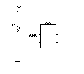
A simple source for a 0-5V analog level is a potentiometer (a.k.a. trimpot). One use is as an easily adjustable variable value to control operation ofyour program, or some gain factors; the kind of thing you might have otherwise done by querying the user in a text window. Here, just turn the pot.
Reading a phototransistor
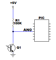
A typical circuit for reading light intensity with a phototransistor is shown at right. Greater light level causes a lower voltage at pin AN0, and a lower value read by the PIC's ADC.
Amplification and level shifting
The above circuit used a sensor without amplification, and the output voltage range was intrinsically limited to 0-5V by the supply rails of the circuit. If you wish to use an opamp or instrumentation amp to produce the voltage to be digitized, you will need to limit it to the 0-5V range, and possibly also to level-shift it so that both polarities of sensing are readable. There are many ways to accomplish these things.
The best way is to use a level of 2.5V as your "null" level. If you use a rail-to-rail opamp (for example, see the circuits below) with supply rails of 0 and 5V, its output is naturally limited to the PIC's analog input range.
Amplified phototransistor
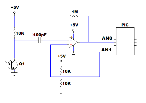
Above is an amplified phototransistor circuit, which provides 100-fold gain (1M/10K) and a high-pass filter with a time constant of 1mS (10Kohm * 100pF). Thus it responds sensitively to a rapid change in light level, probably caused by a strobed LED or IRED, while ignoring overall (DC) light level.
Strobing an LED or IRED briefly (e.g. 100uS) and infrequently (e.g. every 5 mS) allows you to use 10x the rated steady current, and get 10x more light, without overheating the LED. It also allows you to use a phototransistor circuit that responds only to changes, and your PIC software can compare the light level just before and during the flash. All of these allow greatly improved sensitivity.
The chip is a high-speed rail-to-rail opamp such as LM6132, with supply rails of 0 and 5V. Its non-inverting input is held at 2.5V by the voltage divider, and therefore this is the quiescent level of the inverting input as well -- and of the output. The ADC in 10-bit mode reads about 512.
Perhaps the voltage divider produces not exactly 2.5V, or the ADC maps 2.5V not to exactly half scale? The connection from the 2.5V reference point to analog input AN1 allows the PIC to determine the ADC result corresponding to quiescence.
tip - high gain high speed opamp circuits are often unstable, as you can observe with an oscilloscope (and only with an oscilloscope). Try to eliminate oscillations with a small capacitor (e.g. 10pF) across the feedback resistor (1M here). Always use a supply decoupling capacitor (e.g. 0.1uF) across the supply rails, right near the chip.
Instrumentation amp
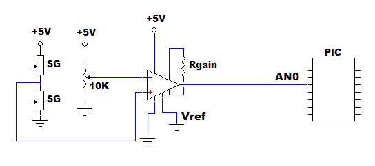
Instrumentation amps are often used with full- or half- strain gauge bridges (four or two strain gauge elements). A half-bridge is shown above. The gain of the instrumentation amp is set by a gain resistor according a to a formula in the datasheet, typically gain = 50K/Rgain.
For easy interfacing to a PIC's 0-5V analog input range, use a rail-to-rail instrumentation amp such as AD623. The instrumentation amp subtracts its two inputs, multiplies the difference by the gain, and adds on the reference voltage. Here we've used a reference voltage of zero, but we could have made it 2.5V by using a voltage divider. With a reference voltage of zero, which is preferable, how can we read deflections of the strain gauge bridge of both polarities? The 10K nulling trimpot allows us to set the quiescent output of the instrumentation amp to 2.5V.
Often strain gauges need an amplification factor of 500 or even 1000. At these high gains, noise from nearby digital devices (such as a PIC) can cause erratic operation of the amplifier. Use supply decoupling capacitors (typically 0.1uF) near the chip, from both supply rails to Vref (ground here). If it is acceptable to low-pass the signal, use an appropriate capacitor between the inverting and non-inverting inputs of the instrumentation amp (e.g. for a 1mS low pass, C=0.1uF here, because 0.1uF * 10Kohm = 1mS). You can also use an RC low pass between the output of the instrumentation amp and the PIC input. In many cases you may need to use a standalone strain gauge amplifier board with its own power supply.
Code
You can include code as shown below. I find that the code has to be indented at least one space to prevent wiki interpretation of the pound sign # at the beginning of a line, and other unexpected behavior.
/*
  AnalogInput.c m.peshkin 2007-12-24
  Range of input voltages on pins AN0 to AN11 is 0 to 5 volts only.
  This maps to 0-255 ADC values if ADC is in 8 bit mode,
  or to 0-1023 ADC values if ADC is in 10 bit mode.
  There is only one ADC, with a switch to connect it to up to 12 input pins named AN0 to AN11.
  After you switch inputs, wait 10uS for the ADC to settle onto the new input
*/

#include <18f4520.h>
#DEVICE ADC=10                   // set ADC to 10 bit accuracy, or it could be just 8
#fuses HS,NOLVP,NOWDT,NOPROTECT
#use delay(clock=20000000)

int16 value;      // if you selected 10 bit accuracy, don't use an 8 bit int

void main() {
  setup_adc_ports(AN0_TO_AN3);             // Enable analog inputs; choices run from just AN0, up to AN0_TO_AN11
  setup_adc(ADC_CLOCK_INTERNAL);      // the range selected has to start with AN0
  set_adc_channel(0);         // there's only one ADC so select which input to connect to it; here pin AN0
  delay_us(10);                    // wait 10uS for ADC to settle to a newly selected input
  while (TRUE) {
    value = read_adc();         // now you can read ADC as frequently as you like
    output_d(value>>2);      // on port D show only the most significant 8 of the 10 bits; tricky >> means shift right 2 bits
    output_bit(PIN_C0, (value & 2)>>1);    // display the two least significant bits; tricky & is bitwise AND
    output_bit(PIN_C1, (value & 1));
    delay_ms(10);
  }
}
