Difference between revisions of "PIC32MX: SPI EEPROM"
MeganWelker (talk | contribs) |
MeganWelker (talk | contribs) (→Code) |
||
| Line 26: | Line 26: | ||
Where possible, make it a single piece of well-commented cut-and-pastable code, or at least make each function that way, so others can easily copy it. Most comments should be in the code itself; outside the code (on the wiki) should only be explanatory comments that are too cumbersome to include in the code. |
Where possible, make it a single piece of well-commented cut-and-pastable code, or at least make each function that way, so others can easily copy it. Most comments should be in the code itself; outside the code (on the wiki) should only be explanatory comments that are too cumbersome to include in the code. |
||
// This code checks the writing and reading of an EEPROM via SPI communication. Note: using this |
|||
code, one can verify using the scope that the EEPROM can actually be read and the read content is just |
|||
what is written into. |
|||
//this code also tells us that the transition between "write" and "read" is big. As a clock pulse is about |
|||
several us(even with prescaler set to 1024), the transition is about ms. So in this case, |
|||
//if new data is written, and you read it soon afterwards(us), the EEPROM will not respond. |
|||
//note: lines of code like "//int mData=SPI2STAT;" is used to read the status register to debug |
|||
#include "Compiler.h" |
|||
#include "HardwareProfile.h" |
|||
#include <plib.h> |
|||
#include "LCD.h" |
|||
#define chipselect LATCbits.LATC1 |
|||
//manipulate /CS of EEPROM. Manipulation of EEPROM cannot be done by linking /SS of PIC and /CS of ROM. One |
|||
can check this with a scope: built-in functions like SpiChnPutc() does not generate corresponding |
|||
chipselect signal |
|||
int main() |
|||
{ |
|||
lcd_init(); |
|||
mInitAllLEDs(); |
|||
LATC |= 0b0000000000000010; //Use C1 of PIC to toggle /CS of ROM |
|||
TRISC &=0b1111111111111101; //intialize C1 as output |
|||
TRISGbits.TRISG7=1;// set G7 as digital input |
|||
char LCDbuffer[33]; // this will store the string for the LCD |
|||
int ENA= 0b00000110; //ROM write-enable instruction |
|||
int INS1=0b00000010; //ROM write instruction |
|||
int add1=0x00; //address byte 1 |
|||
int add2=0x11; //address byte 2 |
|||
int add3=0xee; //address byte 3 |
|||
int INS2=0b00000011; //ROM read instruction |
|||
int INS3=0b00000101; //read status register |
|||
int DIS = 0b00000100; //write disable sequence |
|||
while(1) //include a while loop to examine with a scope(cannot run single when there is 5ms time lag) |
|||
{ |
|||
IEC0CLR=0x03800000; //disable all interrupts |
|||
SPI2CON = 0; //resets SPI2 |
|||
int dump=SPI2BUF; //clears the receive buffer |
|||
IFS0CLR=0x03800000; //clear any existing event |
|||
SPI2STATCLR=0x40; //clears overflow flag |
|||
SpiChnOpen(2,SPI_CON_MSTEN| SPI_CON_MODE8|SPI_CON_ON, 1024); // divide fpb by 1024, configure the I/O ports. |
|||
//there is another way to open SPI channel, but essentially the same, intialize the SFRs |
|||
Delayus(50); |
|||
chipselect=0; //enable chip. the ROM starts up with /CS high |
|||
SpiChnPutC(2,ENA); |
|||
Delayus(100); //give enough time for the previous instruction to get executed |
|||
chipselect=1; //toggle /CS to properly set write enable, demanded by the ROM |
|||
Delayus(50); |
|||
Delayus(30); |
|||
chipselect=0; //enable chip again to initiate write sequence |
|||
Delayus(50); |
|||
SpiChnPutC(2,INS1); |
|||
SpiChnPutC(2,add1); |
|||
SpiChnPutC(2,add2); |
|||
SpiChnPutC(2,add3); |
|||
SpiChnPutC(2,0x50); |
|||
//the previous five instructions writed byte 0x50 to address(1+2+3) |
|||
Delayus(200); // delay long enough for the sequence to be fully executed |
|||
chipselect=1; //deselect the chip to enable internal write sequence which is surprisingly slow!! |
|||
Delayus(5000); //yes! believe your eyes, 5ms. otherwise the chip would be 'busy' so that the following read sequence is 'dumped' |
|||
chipselect=0; //select chip to initiate reading |
|||
Delayus(50); |
|||
SpiChnPutC(2,INS2); |
|||
//reading instruction |
|||
SpiChnPutC(2,add1); |
|||
SpiChnPutC(2,add2); |
|||
SpiChnPutC(2,add3); |
|||
//read sequence, to read the very place where data was written |
|||
//int mData=SPI2STAT;//841 if put here |
|||
SpiChnPutC(2,0x00); |
|||
//this line is necessary since the ROM needs clock signal to clock out the data. |
|||
//the reset of this code is hardly necessary for one to observe the write and read is executed. Because using a scope, one can observe the data is clocked out of the EEPROM the moment the address is given(so fast!) |
|||
//when this line is excuted, the data is put onto the SDI pins of PIC and as one bit is shifted out of SDO, a new bit is shifted into SDI |
|||
//int mData=SPI2STAT; //841 here |
|||
while(SPI2STAT!=0x849){} //wait until the TX buffer is empty, and enable data storage by clearing overflow flag!!! |
|||
//and this is the TRICKY part,without this line, one can get only 0xff |
|||
//int mData=SPI2STAT; //849 here, transmit is empty |
|||
SPI2STATCLR = 0x40; //clear overflow flag |
|||
int receive = SPI2BUF; //since overflow is cleared, buffer is read so that new data can come in |
|||
//int mData=SPI2STAT; //808 here: busy and buffer is cleared, new data should be waiting to come in |
|||
Delayus(500); |
|||
int mData=SPI2STAT; //9 here, |
|||
receive = SPI2BUF; //read |
|||
Delayus(200); |
|||
chipselect=1; //end of reading sequence |
|||
sprintf(LCDbuffer, "\f%c", receive); // make the string 0x50 represents "P" in ASCII |
|||
putsLCD(LCDbuffer); // write the contents of the variable |
|||
} |
|||
} |
|||
== Further Reading == |
== Further Reading == |
||
Revision as of 00:18, 16 February 2010
Original Assignment
Do not erase this section!
Your assignment is to interface to the SPI 25AA1024 EEPROM chip.
Overview
You can use the PIC32 to communicate with an EEPROM chip using SPI. The EEPROM chip can store data sent from the PIC and be retrieved at a later time (like an external hardrive).
To test that the code data was writing and reading correctly, the attached code sends data to the EEPROM through SPI, then from the EEPROM back to the PIC, and out to a LED display screen.
Circuit
Include a schematic and give any part numbers. A photo of your circuit is OK, but not as a replacement for a schematic.
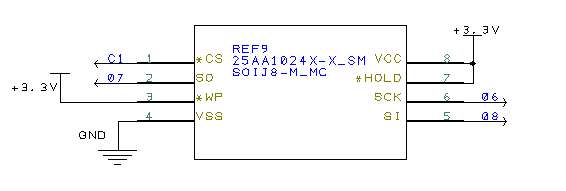
Connection schematic for 25AA1024 chip
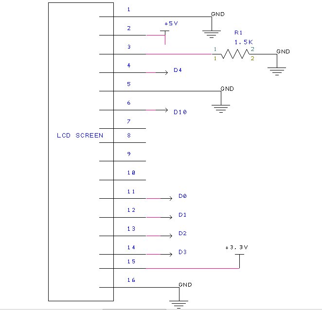
For visual feedback the PIC32 was connected to and LCD screen(1602A1 USB-A/Mini-B5-06):
Code
Where possible, make it a single piece of well-commented cut-and-pastable code, or at least make each function that way, so others can easily copy it. Most comments should be in the code itself; outside the code (on the wiki) should only be explanatory comments that are too cumbersome to include in the code.
   // This code checks the writing and reading of an EEPROM via SPI communication. Note: using this
     code, one can verify using the scope that the EEPROM can actually be read  and the read content is just
     what is written into.
   //this code also tells us that the transition between "write" and "read" is big. As a clock pulse is about
     several us(even with prescaler set to 1024), the transition is about ms. So in this case,
   //if new data is written, and you read it soon afterwards(us), the EEPROM will not respond.
   //note: lines of code like "//int mData=SPI2STAT;" is used to read the status register to debug
     #include "Compiler.h"
     #include "HardwareProfile.h"
     #include <plib.h>
     #include "LCD.h"
     #define      chipselect     LATCbits.LATC1
   //manipulate /CS of EEPROM. Manipulation of EEPROM cannot be done by linking /SS of PIC and /CS of ROM. One
     can check this with a scope: built-in functions like SpiChnPutc() does not generate corresponding
     chipselect signal
int main()
{
  lcd_init();
  mInitAllLEDs();
  LATC |=   0b0000000000000010;		//Use C1 of PIC to toggle /CS of  ROM
  TRISC &=0b1111111111111101;		//intialize C1 as output

  TRISGbits.TRISG7=1;// set G7 as digital input
char LCDbuffer[33]; // this will store the string for the LCD
int ENA= 0b00000110; //ROM write-enable instruction int INS1=0b00000010; //ROM write instruction int add1=0x00; //address byte 1 int add2=0x11; //address byte 2 int add3=0xee; //address byte 3 int INS2=0b00000011; //ROM read instruction int INS3=0b00000101; //read status register int DIS = 0b00000100; //write disable sequence while(1) //include a while loop to examine with a scope(cannot run single when there is 5ms time lag) {
IEC0CLR=0x03800000; //disable all interrupts SPI2CON = 0; //resets SPI2 int dump=SPI2BUF; //clears the receive buffer IFS0CLR=0x03800000; //clear any existing event SPI2STATCLR=0x40; //clears overflow flag
SpiChnOpen(2,SPI_CON_MSTEN| SPI_CON_MODE8|SPI_CON_ON, 1024); // divide fpb by 1024, configure the I/O ports. //there is another way to open SPI channel, but essentially the same, intialize the SFRs Delayus(50); chipselect=0; //enable chip. the ROM starts up with /CS high
SpiChnPutC(2,ENA);
Delayus(100); //give enough time for the previous instruction to get executed chipselect=1; //toggle /CS to properly set write enable, demanded by the ROM Delayus(50); Delayus(30); chipselect=0; //enable chip again to initiate write sequence Delayus(50); SpiChnPutC(2,INS1); SpiChnPutC(2,add1); SpiChnPutC(2,add2); SpiChnPutC(2,add3); SpiChnPutC(2,0x50); //the previous five instructions writed byte 0x50 to address(1+2+3)
Delayus(200); // delay long enough for the sequence to be fully executed chipselect=1; //deselect the chip to enable internal write sequence which is surprisingly slow!!
Delayus(5000); //yes! believe your eyes, 5ms. otherwise the chip would be 'busy' so that the following read sequence is 'dumped'
chipselect=0; //select chip to initiate reading
Delayus(50);
SpiChnPutC(2,INS2);
//reading instruction
SpiChnPutC(2,add1);
SpiChnPutC(2,add2);
SpiChnPutC(2,add3);
//read sequence, to read the very place where data was written
//int mData=SPI2STAT;//841 if put here
SpiChnPutC(2,0x00);
//this line is necessary since the ROM needs clock signal to clock out the data.
//the reset of this code is hardly necessary for one to observe the write and read is executed. Because using a scope, one can observe the data is clocked out of the EEPROM the moment the address is given(so fast!)
//when this line is excuted, the data is put onto the SDI pins of PIC and as one bit is shifted out of SDO, a new bit is shifted into SDI
//int mData=SPI2STAT; //841 here while(SPI2STAT!=0x849){} //wait until the TX buffer is empty, and enable data storage by clearing overflow flag!!! //and this is the TRICKY part,without this line, one can get only 0xff
//int mData=SPI2STAT; //849 here, transmit is empty SPI2STATCLR = 0x40; //clear overflow flag int receive = SPI2BUF; //since overflow is cleared, buffer is read so that new data can come in //int mData=SPI2STAT; //808 here: busy and buffer is cleared, new data should be waiting to come in
Delayus(500); int mData=SPI2STAT; //9 here,
receive = SPI2BUF; //read
Delayus(200);
chipselect=1; //end of reading sequence
sprintf(LCDbuffer, "\f%c", receive); // make the string 0x50 represents "P" in ASCII
putsLCD(LCDbuffer);  // write the contents of the variable
}
}

