Waveform Generation with AD9833, and SPI
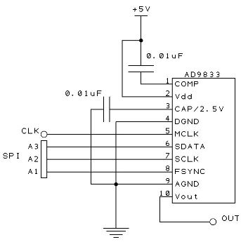
The AD9833 is a programmable waveform generator capable of creating sine, triangular, or square wave outputs in a frequency range of 0 to 12.5 MHz. It has two 28-bit frequency registers and two 12-bit phase registers that can be written to and output from the VOUT pin. This chip is perfectly suited for use with the PIC 18F4520, as it uses SPI communication for its setup and control. A connection diagram for the AD9833 is given to the right. The MCLK pin is tied directly to the oscillator of the PIC, and the three SPI communication lines are connected to three I/O pins on the PIC (in this case pins A1, A2, and A3).
In order to establish communication between the PIC and the AD9833, we need to set up the SPI for the pins we wish to use. The following code should be included in your program.
#use spi(DO = PIN_A3, CLK = PIN_A2, ENABLE = PIN_A1, BITS = 16, MASTER, ENABLE_ACTIVE = 0, MSB_FIRST, IDLE = 1)
The first three arguments determine which three pins we will be using: DO is the "SDATA" pin of the AD9833, CLK is the "SCLK" pin, and ENABLE is the "FSYNC" pin. The next argument states that the max number of bits in one transfer is 16. The next argument specifies that the PIC is the master and the AD9833 is the slave. The AD9833's FSYNC pin is active low, and it accepts the most significant bit (MSB) of each transfer first. The SCLK pin is also specified to be kept high when not in use. After this initial setup, the SPI communication is quite straightforward. We simply use the function spi_xfer() whenever we want to send information via SPI to the AD9833.
Now that we can talk to the waveform generator, we need to know what it needs to be told to produce what we want. Each of the 16 bits transferred has a meaning, and these meanings are described in the Table below. Note that the if a frequency register is being written to (first two bits = 01 or 10), the last 14 bits are the value of the write, and do not have the same meaning as specified in the table. Similarly, if a phase register is being written to (first two bits = 11), the last 12 bits are the value of the write. Only if the control register is being written to (first two bits = 00) are most of the meanings specified in the table applicable.
| Bit | Significance |
|---|---|
| D15,D14(MSB) | 10 = FREQ1 write, 01 = FREQ0 write, 11 = PHASE write, 00 = control write |
| D13 | If D15,D14 = 00, 0 = individual LSB and MSB FREQ write, 1 = both LSB and MSB FREQ writes consecutively |
| If D15,D14 = 11, 0 = PHASE0 write, 1 = PHASE1 write | |
| D12 | 0 = writing LSB independently, 1 = writing MSB independently |
| D11 | 0 = output FREQ0, 1 = output FREQ1 |
| D10 | 0 = output PHASE0, 1 = output PHASE1 |
| D9 | Reserved. Must be 0. |
| D8 | 0 = RESET disabled, 1 = RESET enabled |
| D7 | 0 = internal clock is enabled, 1 = internal clock is disabled |
| D6 | 0 = onboard DAC is active for sine and triangle wave output, 1 = put DAC to sleep for square wave output |
| D5 | 0 = output depends on D1, 1 = output is a square wave |
| D4 | Reserved. Must be 0. |
| D3 | 0 = square wave of half frequency output, 1 = square wave output |
| D2 | Reserved. Must be 0. |
| D1 | If D5 = 1, D1 = 0. Otherwise 0 = sine output, 1 = triangle output |
| D0 | Reserved. Must be 0. |
Obviously this is a lot of information to pass to the waveform generator, but this setup can be performed with only a few SPI transfers. This is nearly all you need to know to set the AD9833, but there are two more critical relationships:
In other words, the output frequency and phase shift are not the values of the frequency or phase registers. They are related by the above equations, so the values you send to the registers need to be modified from the actual frequency and phase shift. For instance, if we sent 200 to the FREQ register and 100 to the PHASE register, and we were using a 20 MHz MCLK, we would output a 14.9 Hz wave with a phase shift of 0.15 radians.
In order to setup or update the AD9833 you first need to reset it, then transfer the frequency and phase information, then "unreset" it. For example, if we wanted to output a 20 kHz square wave with no phase shift, we would send the following:
spi_xfer(0b0010000101101000);


