Phase-Sensitive Detection
Overview
One effective way to recover the small signal buried by large ambient noise is to use the so called phase sensitive detector, or lock-in amplifier. A phase sensitive detector achieves narrow bandwidth amplification by reducing the noise content at falling outside the interested bandwidth.
When the noise is white in nature, we can reduce its level of magnitude dramatically by limiting the bandwidth of detection, which includes the frequency occurring to the signal while excludes the frequencies occurring to the noise. Phase sensitive detection enables extremely narrow bandwidth detection (0.001Hz is normal). Typical application scenario is using electric transducers where the amplitude of noise is in mili volts and the signal falls into nano volt region. Sophisticated phase sensitive detector can extract signals buried in noise that is times larger in magnitude.
In this article, we focus on a quick and easy method of building a phase sensitive detector from op-amps and analog switches.
Mathematical model
Consider two signals, and , where ,
Then, the product of and is:
Let’s integrate the product over time :
When , both parts are equal to 0, except when and , the integration result is equal to .
As can be observed, only signals in phase, in other words, sharing the same frequency and phase angle, will result in a non-zero value after multiplication and integration. This indicates a way to recover the signal from noise: by modulating the interesting signal and doing the maths.This is the mathematical foundation of phase sensitive detection, because all signals can be broken down in to several harmonic components.
Method
A phase sensitive detection can be split into 6 stages:
1. Modulation: Modulate the signal at a certain frequency.
2. Pre-amplification: A high-speed amplifier required to amplify the signal (along with the noise) to a suitable level for succeeding circuit. We can also stick in a high pass filter (can be a capacitor) after amplification, just to eliminate the DC portion of the noise.
3. Reference circuit: Usually a pulse wave at the modulating frequency, which can be from a function generator, or a 555 timer, or PIC, etc.
4. Multiplier: At this stage, we multiply the pre-amplified signal (along with the noise) with the reference signal. One easy way to do multiplication is suggested here: we use the reference signal to turn on and off an analog switch periodically, and let the modulated input signal pass the analog switch. So when the switch is ON (meaning connected to the input pin of the integrator), the output is ‘’, and when the switch is OFF (meaning connected to the ground), the output is ‘’.
5. Integrator (demodulation): Let the multiplied signal pass through an integrator. The multiplied signal can have a lot of components – almost all of them will become zero after integration (see explanation in the mathematical model), but the one which is the product of the modulated signal and the reference signal will remain, because they are at the same frequency and the same phase angle. This is the essence of phase sensitive detection – only the product of the two signals that are ‘in phase’ will remain after integration. ‘In phase’ means the two signals share common frequency and phase angle. We can also do amplification at the integration stage by sticking in a feedback resistor (see the example circuit diagram), just for convenience.
6. Low pass filter: After integration, the signal is recovered and demodulated to a DC output. However, it may not be a perfect DC voltage due to high frequency spikes that still exist. That’s why the low pass filter come into play.
Example Circuit
The concept of phase sensitive detection has been proved effective in optical tracking with lateral effect photodiode. The following circuit picks up the difference of the two corresponding output pins of the photodiode, in order to tell the position of the centroid of IR light on the photodiode sensing surface. The connection for the Y+ and Y- pins of the photodiode is exactly the same with what’s shown here for X+ and X-. The timer is realized by a 555 chip, and the chip for analog switch is Max4526.
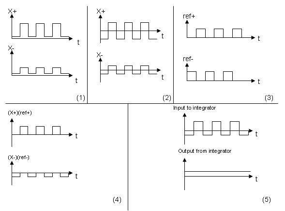
Here is an illustration of the working principle of the example circuit.
(1)The magnified signal from the X+ and X- pins of the photodiode.
(2)Signals after high pass filter.
(3)Reference signals for X+ and X- respectively.
(4)Signals after multiplying with reference signals.
(5)Signals before and after integration.
Commercial phase sensitive detectors
This link below provides some useful information on commercially available phase sensitive detectors, or lock-in amplifiers.
[1]SRS series Lock-in amplifiers: http://www.thinksrs.com/products/SR810830.htm


![{\displaystyle =-{\frac {AB}{2}}\times {cos[(\omega _{1}+\omega _{2})t+\phi ]-cos[(\omega _{1}-\omega _{2})t-\phi ]}}](https://wikimedia.org/api/rest_v1/media/math/render/svg/c16297ab472330e232f91edb45dca34472d795ed)


![{\displaystyle ={\frac {1}{T}}\int _{0}^{T}-{\frac {AB}{2}}\times \{cos[(\omega _{1}+\omega _{2})t+\phi ]-cos[(\omega _{1}-\omega _{2})t-\phi ]\}\,dt}](https://wikimedia.org/api/rest_v1/media/math/render/svg/085897a67476129152d5f7e97a0b407ce529b205)
![{\displaystyle =-{\frac {AB}{2T}}\int _{0}^{T}cos[(\omega _{1}+\omega _{2})t+\phi ]\,dt+{\frac {AB}{2T}}\int _{0}^{T}cos[(\omega _{1}-\omega _{2})t-\phi ]\,dt}](https://wikimedia.org/api/rest_v1/media/math/render/svg/531816c14da3ee3e28cc467e2ecd4d4c14db87d0)


