LED Drivers


Overview
Large numbers of LEDs in an array (of any size) can be controlled efficiently with the use of LED drivers and demultiplexers.
LED Drivers
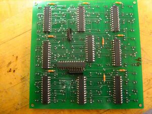
[LED displays can be created using Serial-Input Constant-Current Latched LED Drivers (Made by Allegro, A6278 or A6279). The A6278 outputs to 8 LEDs using 8 NPN constant-current sink drivers, while 16 drivers in the A6279 can control 16 LEDs. Each device includes a CMOS shift register, accompanying data latches and sink drivers.
In this setup, the LEDs are tied high, (+ side connected to Vcc while the negative end is connected to the chip) and the active signal output of the chip is low, creating a voltage difference across the LED. The current through each LED is set by the selection of an external current-control resistor (REXT). The value of this resistor can be determined by formulas in the data sheet, but may also require experimentation for larger displays.
Data
Data is sent from the PIC to the LED driver via the Serial Data line. Within the LED driver data enters into a shift register, filled is then triggered sending the contents of the register to the 8 or 16 LEDs. More specifically; the Serial Data input is passed to the next significant bit in the shift register on each rising edge of the Clock input. When the Latch Enable Input is set high, the contents of the shift register are passed to the latch. If the Output Enable input is low, the contents of the latch are sent to the LED drivers.
Addressing Scheme
Up to 16 LED driver devices (equivalent to 256 LEDs with the A6279) can be controlled with the use of a PIC and a 4- to 16-Line Demultiplexer. Signals from the PIC: Output Enable, held low, allows the data to be passed from the latches to the drivers. The Serial Data line distributes the same data stream to each driver device. A 4-bit address for the desired driver device is sent to the demultiplexer to determine which driver is controlled. The output signal from the demultiplexer to each driver device acts as its Clock input. A clock pulse is sent from the PIC to enabling the demultiplexer, thus the output from the demultiplexer is a clock signal which is then sent to the driver device. This clock signal allows the current Serial Data input bit to be passed to its shift register, data enters and shifts into the shift register on the rising edge of the clock. Once 16 data bits have been passed into the shift register, of the addressed driver device, the Latch Enable signal is sent from the PIC to all of the driver devices. This passes the data from the shift register to the latch and from the latch to the LED drivers, updating 16 LEDs at a time. Output Enable from the driver must be low for the data to be passed to the latch and the LEDs. The outputs of the driver devices which were not being addressed (through the demultiplexer) will remain unchanged, as the data in their shift registers was not updated. Hence, 16 LEDs (one driver device) are updated at a time.
One way to further increase the number of LEDs controlled by the PIC is to employ a 3- to 8-Line Demultiplexer between the PIC and the 4-16 Demultiplexers. Thus, it is possible to control up to 8, 4-16 demultiplexers, which each control up to 16 LED drivers. An additional 3 address bits must be sent by the PIC to this primary demultiplexer to enable one of the (up to) 8 4-16-Line demultiplexers. This scheme allows for the control of up to 2048 LEDs. A sample circuit diagram is shown below.
Example Code
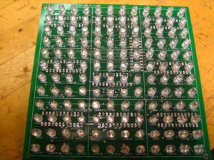
Below is some sample code from the ME 433 Led Cube project. This code updates the LED banks (one driver device = 16 LEDs) which have been flagged. In this example there are 9 banks on each of 6 “sides”, where a side corresponds to the all of LED banks (9 banks, 9 led drivers, 144 LEDs) under the control of a single 4-16 line demultiplexer. An 3-8 line demultiplexer selects the side, or the correct 4-16 demultiplexer. A 2-D array, FLAG, indicates which banks need to be updated. A 2-D array, DATA, contains the 16 bits of data for each bank, the data stream for each driver.
void reset(void) {
for(s=0;s<6;s++) //for each side 1 to 6
{
  for(b=0;b<9;b++) //for each bank 1 to 9
  {
     if(FLAG[s][b]) //true is flagged for change
     {
        ADDY = (s*16) + b;		//4 least significant bits are bank address (sent to 16-Line //demux, 3 most significant bits are the side address (sent to
//8-Line demux)
        output_d(ADDY);	//Set driver device address
        output_low(PIN_B3);  //enable 1 on 8bit demux, held low
        output_low(PIN_B4);  //enable 2 on 8bit demux, held low
        for(i=16;i>0;i--)
        {
           output_low(PIN_B0); // enable 1 on 16 bit demux (clock) is low
           delay_us(10);
           output_bit(PIN_B1,DATA[s*9 + b][i-1]); // sets data
           delay_us(10);
           output_high(PIN_B0); // clock goes high and register records data point
           delay_us(10);
        }
        output_high(PIN_B2); //latch enable high to pass data
        delay_us(10);
        output_low(PIN_B2); //latch enable low to freeze data
   }
  }
}
}