Eagle: Difference between revisions
New page: *UNDER CONSTRUCTION |
first draft of eagle tutorial |
||
| Line 1: | Line 1: | ||
== Overview == |
|||
*UNDER CONSTRUCTION |
|||
[http://www.cadsoftusa.com/ Eagle] is an easy to learn schematic and printed circuit board (PCB) layout editor. It is compatible with Windows, Linux and Mac. Eagle lets the user design a schematic using common electric components, convert it to a PC Board layout, and then automatically rout all of the necessary net connections. The final Eagle layout can then be exported as a CAM file and sent to a PCB manufacturer to order a board. This wiki page describes how to download and effectively operate Eagle. |
|||
== Download == |
|||
A free download to Eagle can be found [http://www.cadsoftusa.com/download.htm here]. Installation guides are provided at the site. Some necessary features may require a license to be activated. Consult your Professor or TA regarding obtaining a license for Eagle. |
|||
== References == |
|||
*[[Media:Eagle_Rules.pdf|Sparkfun Eagle Rules]]: Guidelines for designing and creating PCB layout for manufacture by Sparkfun |
|||
*[[Media:Eagle_Tutorial.pdf|Eagle Tutorial]]: Recommended reading for good overview of Eagle |
|||
*[[Media:Eagle_Manual.pdf|Eagle Manual]]: Full Eagle Manual |
|||
*[[Media:PCBDesignTutorialRevA.pdf|PCB Design Tutorial]]: General tutorial and information on PCB design |
|||
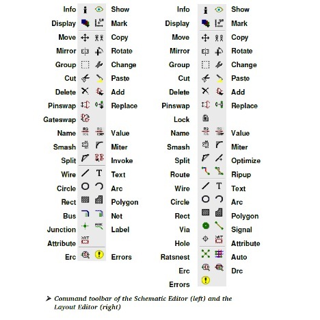
*Button definitions: |
|||
[[Image:EagleCommandList.jpg]] |
|||
== Schematic == |
|||
Before designing the PCB layout, it is essential to first create a schematic of your circuit. In general, the simpler you layout your circuit in the schematic, the easier laying out the PCB will be. Draw the schematic just as you would draw a circuit diagram on paper. |
|||
To draw the schematic, you will need to add the necessary electric components involved in your circuit. Eagle comes with an extensive library of popular components, and a supplemental library of common components used in the Mechatronics classes can be found [[Media:EagleLibrary.zip|here]]. To add the components, click the “ADD” button in the command toolbar and a window will pop up with the aforementioned libraries. The search feature isn’t the best, so it can be useful to try multiple different searches or even manually go through the libraries to find the correct component. The search function does allow for wildcards, (*, ?), so if you know part of the name of a component, you can place an asterisk in the search keyword where you are unsure of the letters or numbers. For example, if you are trying to find the component 74LS00, a search of 74*00* or 74LS00* would yield this component and its variants. Once you’ve found the desired component, click on it and click to place it in the schematic layout sheet. The Esc key will return you to the ADD library to find more components. Pressing the Esc key again will cancel the command. |
|||
Once the components are laid out, it is necessary to connect the pins that go together. It is extremely important that you do NOT use the “Wire” command to connect pins. The correct way to connect pins is to use the “Net” command. After selecting the Net command, you’re your mouse over the connection point of the pin until it connects. If it doesn’t connect, the Net will continue to follow your mouse. |
|||
The Net command doesn’t always connect to the pins, so it is usually necessary to test connections with the move command. If there isn’t a connection, move the component until the desired pin attaches to the Net. Remember, a Net is only connected to a pin if the net is in the connection point of the pin. To display all of the connections, select the display command and display layer 93, pins. Connections are outlined with a green circle. Connections are automatically named. |
|||
If two or more Nets need to be connected, to make sure there is a connection, use the Junction command to create a node between the Nets. If a mistake is made, you can use the undo and redo buttons, or you can use the Delete command to delete components and Nets. |
|||
Once you’ve completed the schematic, you need to check it for errors. Before doing any checks, make sure [[Media:SparkFun.dru|this file]] is saved into your Eagle/dru directory. Then, use the Errors command to find any errors with your schematic. |
|||
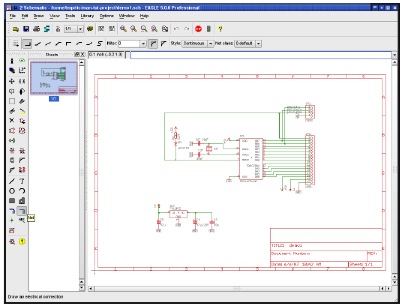
An example of a completed schematic: |
|||
[[Image:EagleSchematic.jpg]] |
|||
== PC Board == |
|||
Once your schematic is completed, you can convert it to a PCB layout by selecting the Board icon . From there, you can layout the components onto a PCB sheet. A nice feature of Eagle is if you don’t change any file names, any further edits to the schematic will update on the PCB layout and visa-versa. As well, both the schematic and PCB layout windows need to be open for this function to work. Either one can be minimized, but not closed. |
|||
In general, it is recommended that PCB layout resembles the schematic and circuit diagram. This way, if there are any errors or you want to make any changes after the board is manufactured, it will be easier to follow the circuit and debug. |
|||
Once all of the components are laid out on the PCB sheet, it is necessary to rout all of the connections. Eagle has a built in autorouter that will do most of the work for you. To autorout the PCB layout, simply select the autorout command. To further customize and optimize the autorout process, refer to the linked Eagle tutorial and manual. |
|||
The autorouter is not perfect, so once it is executed, you will need to go through the layout and make sure that no routs on the same layer (of the same color) are crossing. This would lead to a short circuit. Use the move command to move around routs. If you don’t like the results of the autorouter, you can use the RIPUP command to remove routs. |
|||
If you need to change the properties of or move multiple components together, a useful tool is the Group command. As the name suggests, it will group together selected components so they can all be edited together. |
|||
In general, it’s very useful to label both the components on the PCB as well as component values. To label values of resistors, capacitors and other circuit elements, use the Value command . As well, you can use the Text command to add text noting which component is which on the PCB layout. Make sure to place the text on layer 21, “tPlace.” |
|||
Another useful feature to include on your PCB layout is mounting holes in order to secure your board to your robot. To draw mounting holes, simply use the Hole command. Make sure the hole size is of the correct diameter to mount with screws. |
|||
Once you’ve completed the layout, another error check is necessary. Select the Errors command to check. |
|||
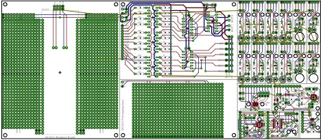
An example of a completed PCB layout. |
|||
[[Image:EaglePCBBreakout.jpg]] |
|||
Once the PCB layout is complete, you’ll need to export it as a CAM file in order for it to be manufactured. Before you begin to export, download this [[Media: sfe-gerb274x.cam|CAM file]] and save it to your Eagle/cam directory. Once the file is saved properly, select the CAM command. Then, select File/Open/Job… and select the CAM file you just downloaded and saved. Finally, select Process Job to complete the process. For more information on customizing the CAM process, refer to the Eagle tutorial and manual. |
|||
Revision as of 13:35, 21 June 2011
Overview
Eagle is an easy to learn schematic and printed circuit board (PCB) layout editor. It is compatible with Windows, Linux and Mac. Eagle lets the user design a schematic using common electric components, convert it to a PC Board layout, and then automatically rout all of the necessary net connections. The final Eagle layout can then be exported as a CAM file and sent to a PCB manufacturer to order a board. This wiki page describes how to download and effectively operate Eagle.
Download
A free download to Eagle can be found here. Installation guides are provided at the site. Some necessary features may require a license to be activated. Consult your Professor or TA regarding obtaining a license for Eagle.
References
- Sparkfun Eagle Rules: Guidelines for designing and creating PCB layout for manufacture by Sparkfun
- Eagle Tutorial: Recommended reading for good overview of Eagle
- Eagle Manual: Full Eagle Manual
- PCB Design Tutorial: General tutorial and information on PCB design
- Button definitions:
Schematic
Before designing the PCB layout, it is essential to first create a schematic of your circuit. In general, the simpler you layout your circuit in the schematic, the easier laying out the PCB will be. Draw the schematic just as you would draw a circuit diagram on paper. To draw the schematic, you will need to add the necessary electric components involved in your circuit. Eagle comes with an extensive library of popular components, and a supplemental library of common components used in the Mechatronics classes can be found here. To add the components, click the “ADD” button in the command toolbar and a window will pop up with the aforementioned libraries. The search feature isn’t the best, so it can be useful to try multiple different searches or even manually go through the libraries to find the correct component. The search function does allow for wildcards, (*, ?), so if you know part of the name of a component, you can place an asterisk in the search keyword where you are unsure of the letters or numbers. For example, if you are trying to find the component 74LS00, a search of 74*00* or 74LS00* would yield this component and its variants. Once you’ve found the desired component, click on it and click to place it in the schematic layout sheet. The Esc key will return you to the ADD library to find more components. Pressing the Esc key again will cancel the command.
Once the components are laid out, it is necessary to connect the pins that go together. It is extremely important that you do NOT use the “Wire” command to connect pins. The correct way to connect pins is to use the “Net” command. After selecting the Net command, you’re your mouse over the connection point of the pin until it connects. If it doesn’t connect, the Net will continue to follow your mouse.
The Net command doesn’t always connect to the pins, so it is usually necessary to test connections with the move command. If there isn’t a connection, move the component until the desired pin attaches to the Net. Remember, a Net is only connected to a pin if the net is in the connection point of the pin. To display all of the connections, select the display command and display layer 93, pins. Connections are outlined with a green circle. Connections are automatically named.
If two or more Nets need to be connected, to make sure there is a connection, use the Junction command to create a node between the Nets. If a mistake is made, you can use the undo and redo buttons, or you can use the Delete command to delete components and Nets.
Once you’ve completed the schematic, you need to check it for errors. Before doing any checks, make sure this file is saved into your Eagle/dru directory. Then, use the Errors command to find any errors with your schematic.
An example of a completed schematic:

PC Board
Once your schematic is completed, you can convert it to a PCB layout by selecting the Board icon . From there, you can layout the components onto a PCB sheet. A nice feature of Eagle is if you don’t change any file names, any further edits to the schematic will update on the PCB layout and visa-versa. As well, both the schematic and PCB layout windows need to be open for this function to work. Either one can be minimized, but not closed. In general, it is recommended that PCB layout resembles the schematic and circuit diagram. This way, if there are any errors or you want to make any changes after the board is manufactured, it will be easier to follow the circuit and debug. Once all of the components are laid out on the PCB sheet, it is necessary to rout all of the connections. Eagle has a built in autorouter that will do most of the work for you. To autorout the PCB layout, simply select the autorout command. To further customize and optimize the autorout process, refer to the linked Eagle tutorial and manual. The autorouter is not perfect, so once it is executed, you will need to go through the layout and make sure that no routs on the same layer (of the same color) are crossing. This would lead to a short circuit. Use the move command to move around routs. If you don’t like the results of the autorouter, you can use the RIPUP command to remove routs. If you need to change the properties of or move multiple components together, a useful tool is the Group command. As the name suggests, it will group together selected components so they can all be edited together.
In general, it’s very useful to label both the components on the PCB as well as component values. To label values of resistors, capacitors and other circuit elements, use the Value command . As well, you can use the Text command to add text noting which component is which on the PCB layout. Make sure to place the text on layer 21, “tPlace.” Another useful feature to include on your PCB layout is mounting holes in order to secure your board to your robot. To draw mounting holes, simply use the Hole command. Make sure the hole size is of the correct diameter to mount with screws. Once you’ve completed the layout, another error check is necessary. Select the Errors command to check.
An example of a completed PCB layout.

Once the PCB layout is complete, you’ll need to export it as a CAM file in order for it to be manufactured. Before you begin to export, download this CAM file and save it to your Eagle/cam directory. Once the file is saved properly, select the CAM command. Then, select File/Open/Job… and select the CAM file you just downloaded and saved. Finally, select Process Job to complete the process. For more information on customizing the CAM process, refer to the Eagle tutorial and manual.
