Difference between revisions of "PCB Artist"
Andrew Long (talk | contribs) |
Andrew Long (talk | contribs) |
||
| Line 131: | Line 131: | ||
[[Image:PCBArtist_Sch_Pins.jpg]] |
[[Image:PCBArtist_Sch_Pins.jpg]] |
||
<br clear=all> |
<br clear=all> |
||
| ⚫ | |||
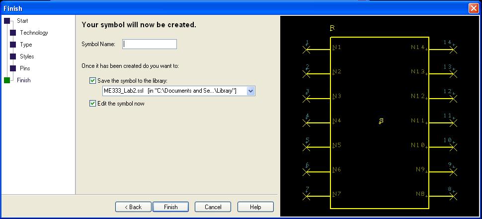
The last window is where you name the symbol and save it to a specific library. |
|||
*Name the component SN74HC04_Inverter and save it in the ME333_Lab2 Library that you downloaded above. |
|||
*Click Finish |
|||
You have now created a schematic symbol. If you checked the 'Edit the symbol now' box, you can see the schematic and edit if you want. We won't do any editting right now though. |
|||
| ⚫ | |||
<br clear=all> |
<br clear=all> |
||
Revision as of 17:55, 7 January 2010
What is a PCB?
A printed circuit board, or PCB, is an epoxy board clad with copper sheets to make electrical connections along fixed routes. A PCB can have many layers of copper and insulator, depending on the complexity of the design. Layers are connected with vias, plated holes maintaining electrical conductivity. A finished PCB is often covered with solder mask, a solder-phobic layer that helps prevent solder bridges, making the PCB green. A white silk screen can be drawn on top of this, used to label the outlines of components and give other critical information. For more information on PCBs, see the wikipedia page Printed Circuit Board.
PCBs are created in a variety of ways. A common method is covering the copper you wish to keep and dipping the board in acid, which etches away the copper you do not want. This method can be done by hand.
A more professional and reliable PCB can be made by designing your circuit in CAD software and ordering the part from a PCB production house. The remainder of this page will describe how to use the proprietary software PCB Artist to design and order a complete PCB.
Advanced Circuits and PCB Artist
Advanced Circuits (www.4pcb.com) is a company based in Colorado known for their quick turn-around and good prices on low volume printed circuit board (PCB) orders. This is the main supplier for PCBs created by students for clasess or research at Northwestern.
Previously, the PCB was created in TraxxMaker or other CAD PCB program, many of which are outdated and difficult to use, then uploaded to Advanced Circuits. Advanced Circuits has created PCB Artist, free software to create schematics and PCBs. This software is designed to order only from Advanced Circuits. This somewhat simplistic software is very intuitive (once comfortable) and allows for simple changes and editing. Additionally, the component library offered is up to date and contains many specific components. This Wiki page will cover the development and ordering process of a simple PCB board.
Contact at Advanced Circuits
Jackie Sartin - Regional Sales Manager
E-mail: jackies@4pcb.com Call: 1-800-979-4PCB (4722) Ext: 1685
Getting Setup
- Have a complete circuit schematic and know exactly what parts (including part numbers) you are using.
- Download the software Or, type “PCB Artist” into google. Then click the download button in the middle of the screen.
- Review the material on this page: Help Guides and User Reference documents
Browse through the Advanced Circuits tutorial pdf to get familiar with the program interface and design process. In general, you will:
- Create a schematic (.sch) that represents the circuit you want to create. This schematic is just like any other schematic you would draw by hand, but it will be used to automate the process of laying out your physical PCB and is very helpful in debugging.
- Create a PCB design (.pcb) that represents your physical PCB, based on your schematic. In this CAD process, the program will automatically grab the components you need and place them outside of the board. You then place each component and connect the pins based on how they are connected in the schematic. The program helps you by highlighting the nets (all the pins that need to be connected) in different colors. You choose how to connect each pin, the width of the copper trace, the layer the copper should be on (top or bottom for a 2 sided board), and the size of the vias. You can have PCB Artist automatically place your components and connect them, but the result may not be pretty or successful.
- Check for errors. Use the Design Rule Check tool to make sure the board is machinable and the pins are connected as they are in your schematic. Carefully scan your board to make sure vias don't accidentally touch traces. Put some silk screen labels next to pins and components, and put your name and the version of your board somewhere for later reference.
- Order your board! Use the student deal ($33 for one board), but note it generally takes a week to make and a few days to ship (another $15). So order early and design carefully.
Some general tips:
- Don't try to make a 2" x 2" board if your space constraints allow for a larger board. It is not worth the effort and possible mistakes trying to squeeze everything into a tiny area if you don't have to.
- Connect your power and ground traces first, they are usually the most complicated.
- Try to keep an organized board. Keep components with many connections close together.
- Use a convention like top layer traces go left-right and bottom layer traces go up-down, this will make routing much easier.
- Give yourself some prototyping area and add extra vias to traces. Thus will allow you some wiggle room when your board arrives and has errors (every board will have some errors!). Traces can be cut with a razor blade fairly easily if the board is not too tight, and can be remade with wires if you remember to leave some extra vias around to solder to.
Download and Installation Instructions
Download and install PCB Artist from Advanced Circuits at the Advanced Artist website. The latest version as of 1/7/2010 is 1.3.2. It is PC only and works best in Windows XP.
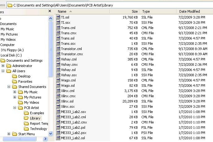
To install a library, download the .zip file from the wiki. Extract the files and place them in the Library folder in the PCB Artist folder the installation makes in your My Documents folder.
Create a Schematic
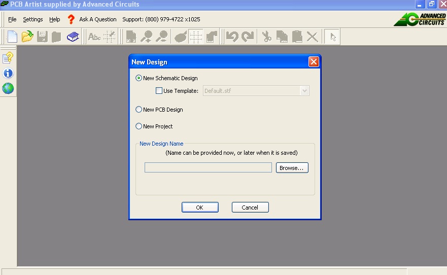
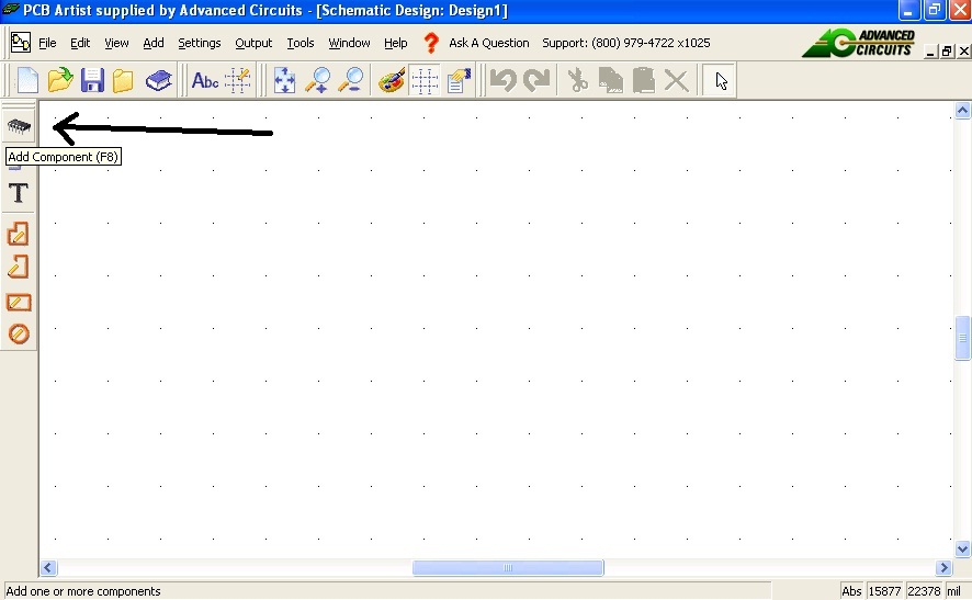
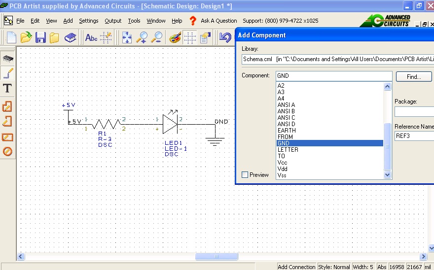
Open a new schematic.
Select Add a Component.
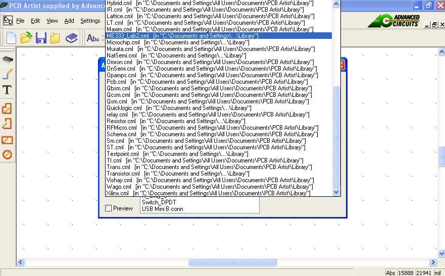
Choose the library your component is in.
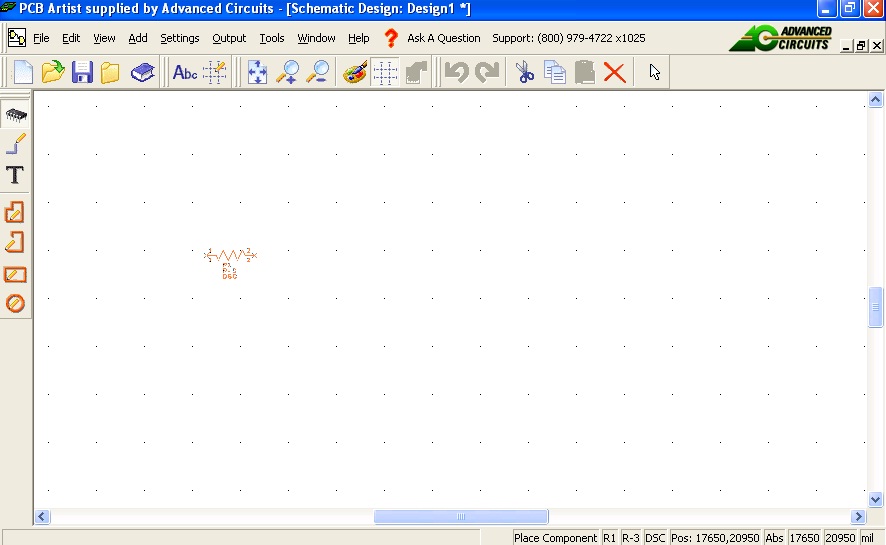
Place the component. Components should be arranged so that the schematic can be read and understood easily, they do not need to be laid out as they would on the PCB, we will do that later.
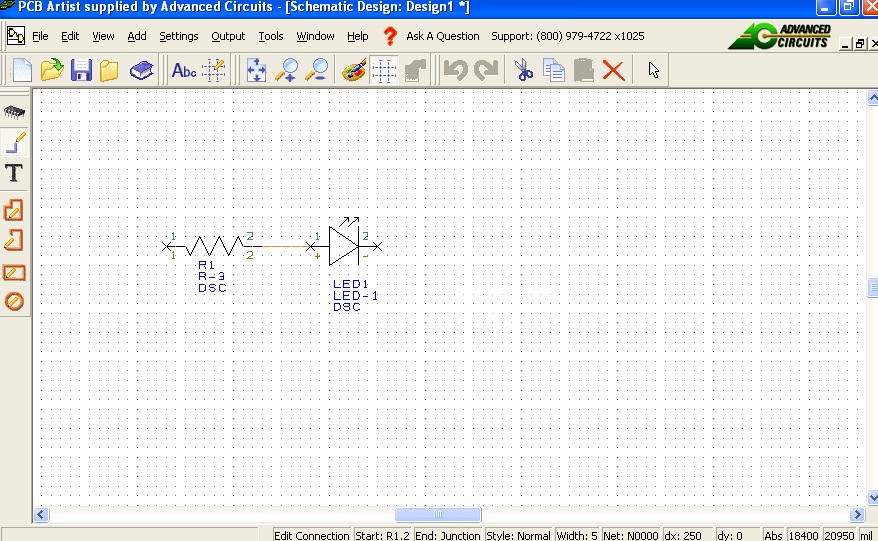
Connect multiple components using the Add Schematic Connection tool. This connection will make it easier to create the PCB. It represents which pins need to be connected on the PCB, but does not represent the actual path the trace will take. We will design that later.
Add a voltage source and ground from the Schema library and connect them to the schematic.
Save the file (.sch). Now we can design a PCB for this circuit.
Create PCB from Schematic
Create a Component
A majority of the time the component you want to use is not in the existing libraries, therefore, you have to create a component. A component consists of a schematic symbol, a pcb symbol and a mapping between the pins of the schematic symbol and the pcb symbol. This section details how to create a component using the SN74HC04 Hex Inverter as an example.
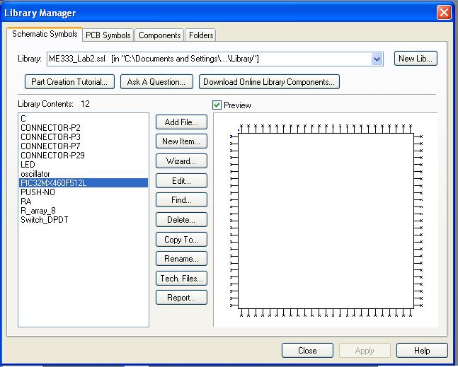
With PCBArtist open (it doesn't matter if any schematics or pcb files are open), click on the blue book at the top of the screen.

This opens the Library Manager of schematic symbols, pcb symbols and components. It will look something similar to the image below.
To make a component, we first need to download the datasheet of the component. Download the datasheet for the Hex Inverter here.
On the first page of the datasheet, we can find a schematic of the component for SN74HC04. We will use this schematic to make our schematic in PCB Artist.
- In PCBArtist, click on the 'Schematic Tab' of the Library Manager.
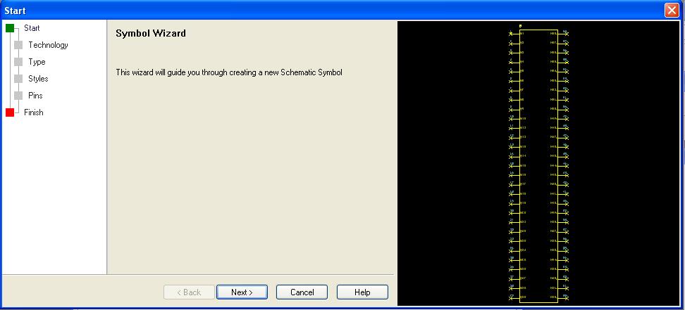
- Click on the 'Wizard' Button in the middle of the window to begin creating a schematic symbol.
This wizard will help you make your schematic symbols.
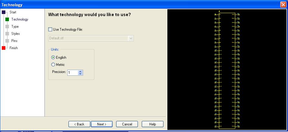
- Click 'Next'
- Choose English with a precision of 1 (these are the units for the symbol)
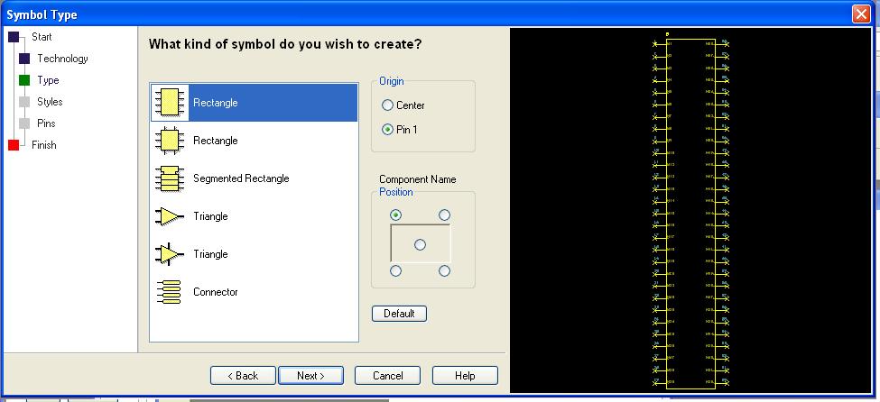
- Next we are going to choose the type of symbol. Our chip has pins on two sides so select the rectangle with pins on two sides (the first one).
- Select the 'center' option for Origin. If you decide to rotate the symbol, it will rotate about this point.
- Select the top left corner for Component Name. This indicates where the component name will be placed.
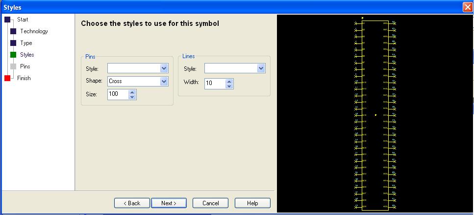
- In the next window, you can choose how you want the pins to be represented, the size of these and the length of the lines going to the pins. Leave these with the default values.
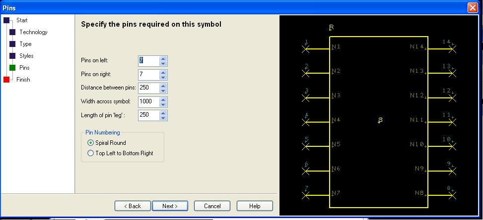
The next window determines the number of pins on each side of the component and some dimensions.
- Enter 7 for both Pins on left and Pins on Right.
- The other dimensions are not as important for the schematic, leave these as the default. (They can be editted later if too big or too small).
- The last part on this page describes how the pins are numbered. Since the schematic on the datasheet spirals the numbers, select the 'Spiral Round' option.
The last window is where you name the symbol and save it to a specific library.
- Name the component SN74HC04_Inverter and save it in the ME333_Lab2 Library that you downloaded above.
- Click Finish
You have now created a schematic symbol. If you checked the 'Edit the symbol now' box, you can see the schematic and edit if you want. We won't do any editting right now though.
