Difference between revisions of "555 Timer"
m |
|||
| Line 1: | Line 1: | ||
__TOC__ |
__TOC__ |
||
==Basic Operation== |
|||
Connection diagram for the 555 IC timer (click for larger image). |
Connection diagram for the 555 IC timer (click for larger image). |
||
| Line 12: | Line 13: | ||
The 555 timer also has a flip-flop, which is controlled by the two comparators and the '''reset''' input. |
The 555 timer also has a flip-flop, which is controlled by the two comparators and the '''reset''' input. |
||
The '''trigger''' and '''reset''' inputs are level-sensitive [[Digital#Active_Low_Input|active low]] inputs. To activate the trigger, the voltage on the ''trigger'' pin must be pulled down to under 1/3 V<sub>CC</sub>. The trigger experiences a delay when it "turns off," so it should be returned to '' |
The '''trigger''' and '''reset''' inputs are level-sensitive [[Digital#Active_Low_Input|active low]] inputs. To activate the trigger, the voltage on the ''trigger'' pin must be pulled down to under 1/3 V<sub>CC</sub>. The trigger experiences a delay when it "turns off," so it should be returned to ''high'' at least 10μs before the end of the timing cycle to avoid double triggering. |
||
To reset the timer, the voltage on the ''reset'' pin must be pulled under 0.4V. The ''reset'' input will override other inputs and set the '''output''' (pin 3) to ''low''. If the ''reset'' input is not going to be used, it should be wired to V<sub>CC</sub> to prevent false signals. |
To reset the timer, the voltage on the ''reset'' pin must be pulled under 0.4V. The ''reset'' input will override other inputs and set the '''output''' (pin 3) to ''low''. If the ''reset'' input is not going to be used, it should be wired to V<sub>CC</sub> to prevent false signals. |
||
Revision as of 18:55, 4 August 2006
Basic Operation
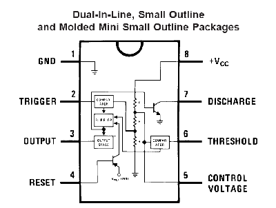
Connection diagram for the 555 IC timer (click for larger image).
See the Datasheet for the LM555 for more information and example applications/circuits.
The output of a 555 timer is either high (close to +VCC) or low (close to GND).
Inside the 555 timer is a voltage divider the divides +VCC into thirds. A voltage comparator compares the trigger input (pin 2) with 1/3 VCC, and another comparator compares the threshold (pin 6) with 2/3 VCC. The point at 2/3 VCC on the voltage divider is connected to the control voltage (pin 5). This pin can be used to modify the values of 1/3 VCC and 2/3 VCC without having to change VCC. However, if this input is not going to be used, it should be connected to a bypass capacitor (0.01uF) to protect it from noise.
The 555 timer also has a flip-flop, which is controlled by the two comparators and the reset input.
The trigger and reset inputs are level-sensitive active low inputs. To activate the trigger, the voltage on the trigger pin must be pulled down to under 1/3 VCC. The trigger experiences a delay when it "turns off," so it should be returned to high at least 10μs before the end of the timing cycle to avoid double triggering.
To reset the timer, the voltage on the reset pin must be pulled under 0.4V. The reset input will override other inputs and set the output (pin 3) to low. If the reset input is not going to be used, it should be wired to VCC to prevent false signals.
In its initial state (assuming threshold is low and trigger is high), the 555 timer's internal flip-flop connects the discharge (pin 7) to the ground and sets the output to low. Each time the trigger voltage is pulled down under 1/3 VCC, the flip-flop will break the discharge pin's connection to ground, and set the output to high. It will hold this state until something (usually a capacitor) forces the threshold pin's voltage equal to 2/3 VCC, which will reset the flip-flop.
Monostable and Astable mode
The 555 family of timer chips can be used in either monostable mode or astable mode. In the monostable or "one shot" mode, each time the 555 timer is triggered, the output will go high for a specified amount of time, then return to low and await another trigger signal. In the astable mode, the timer triggers itself periodically and becomes an oscillator, sending out a train of pulses.
Monostable Mode
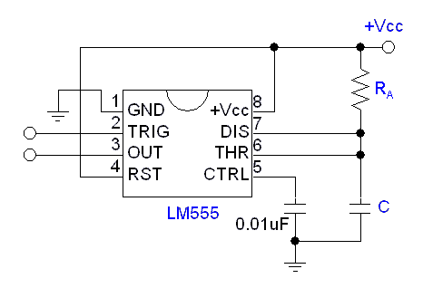
Connections for the 555 timer in monostable mode:
The circuit operates as follows:
- In this circuit's initial condition, the capacitor C is held discharged through the discharge pin, which is grounded through the flip-flop in the timer. The threshold voltage is equal to the voltage across the capacitor.
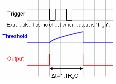
- When the trigger pin receives a negative trigger pulse less than 1/3 VCC, the flip-flop sets the output to high and disconnects the discharge pin from the ground. This allows the capacitor to charge until the voltage across it reaches 2/3 VCC, which takes about t=1.1RAC seconds.
- When the threshold voltage reaches 2/3 VCC, the flip-flop resets, connecting discharge to the ground and setting output to low. It is now back in the initial state, and awaits another trigger pulse.
By selecting the resistor and capacitor, the length of the output pulse can be controlled. If the trigger receives a signal while the output is still high, there is no effect. This circuit can be used for debouncing.
Timing diagram for the 555 in monostable mode:
Astable mode
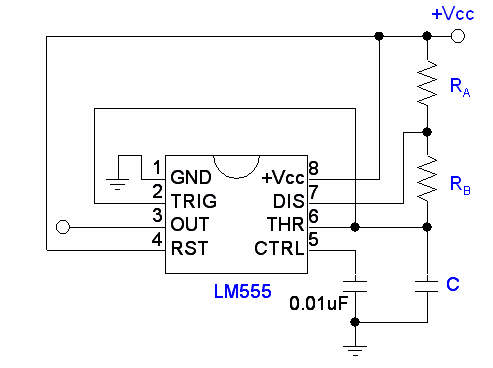
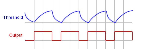
In the astable mode, the circuit will keep re-triggering itself, resulting in a pulse train. The circuit for the 555 in astable mode looks like this:
In this case, the capacitor charges and discharges between 1/3 VCC and 2/3 VCC. The 555's output will the high while charging, and low while discharging. The capacitor charges and discharge at different rate—it has to charge through RA and RB, but it only discharges through RB.
Thus, we can adjust the length of the output's highs and lows by adjusting these resistors.
The length of a output high is equal to:
The length of a output low is equal to:
Each period consists of an output high and output low, so the total period is equal to:
and the frequency is:
The duty cycle, often expressed as a percentage, is defined as the length of the pulse divided by the length of the period:
The timing diagram for the 555 in astable mode:
References
van Roon, Tony. 555 Timer Tutorial'. 5 July 2006. http://www.uoguelph.ca/~antoon/gadgets/555/555.html.
