PIC16F684: Difference between revisions
m →Pinout |
|||
| (9 intermediate revisions by the same user not shown) | |||
| Line 2: | Line 2: | ||
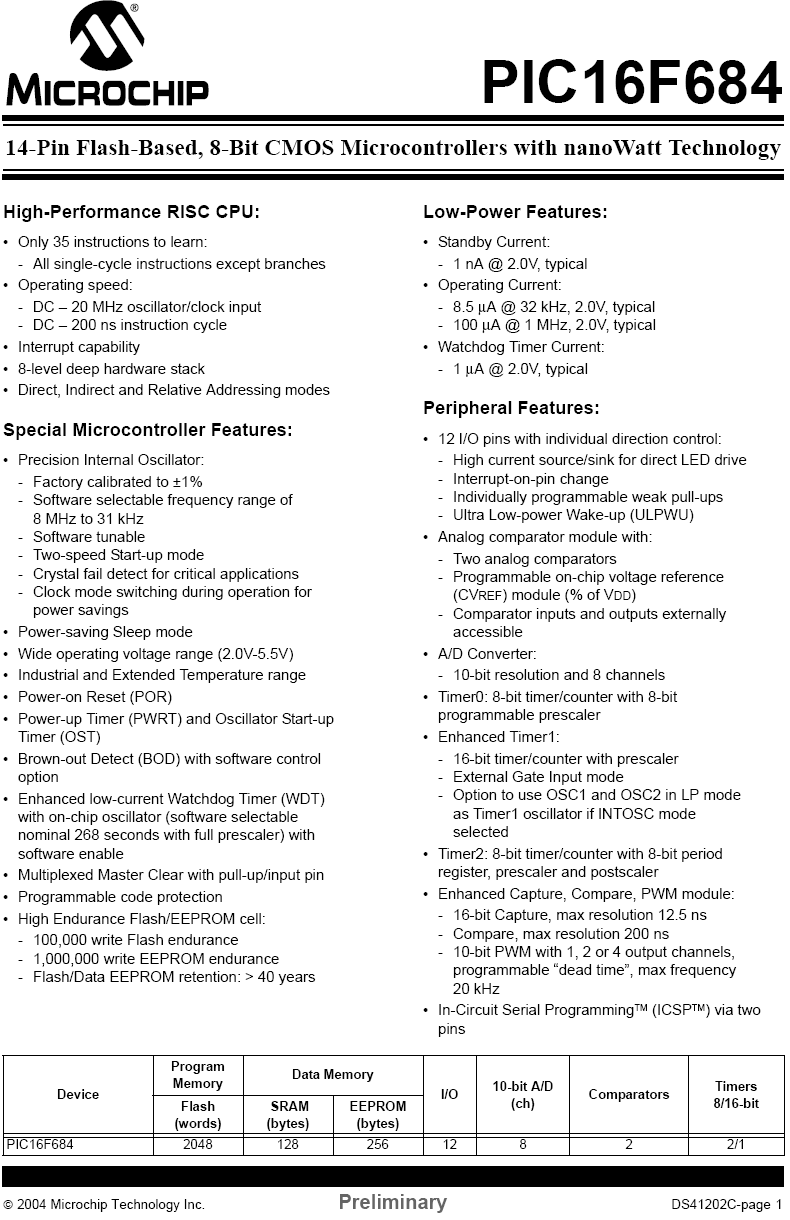
For a complete list of features, see [[media:pic16f684 features.png|this printout]] from the datasheet. |
For a complete list of features, see [[media:pic16f684 features.png|this printout]] from the datasheet. |
||
IMPORTANT: '''See [[PIC16F684 Registers]] for detailed information on registers.''' |
|||
===Pinout=== |
===Pinout=== |
||
| Line 15: | Line 17: | ||
| <math>V_{SS}\,</math> || Ground |
| <math>V_{SS}\,</math> || Ground |
||
|- |
|- |
||
| <math>V_{ |
| <math>V_{REF}\,</math> || External Voltage Reference |
||
|- |
|||
| <math>RA\#/RC\#\,</math> || PORTA/PORTC Programmable I/O |
| <math>RA\#/RC\#\,</math> || PORTA/PORTC Programmable I/O |
||
|- |
|- |
||
| Line 25: | Line 28: | ||
|} |
|} |
||
== |
==Initialization== |
||
==Configuring I/O== |
==Configuring I/O== |
||
This section shows two sections of code that are used for setting up the I/O of the PIC. The INIT_IO function sets up the ports by setting their default value and their direction. The second function, INIT_ADC sets up the A/D converter. |
|||
<pre> |
|||
INIT_IO |
|||
BCF STATUS,RP0 ;Bank 0 |
|||
CLRF PORTA ;Init PORTA - initially set to LOW |
|||
MOVLW B'000101' ;Set RA<0> as input |
|||
MOVWF TRISA ; and set RA<5:1> |
|||
; as outputs |
|||
BSF STATUS,RP0 ;Bank 1 |
|||
CLRF PORTC ;Init PORTC - initially set to LOW |
|||
MOVLW B'000000' ;Set RC<5:0> as outputs |
|||
MOVWF TRISC |
|||
CLRF ANSEL ;Set all pins initially to digital I/O |
|||
MOVLW B'000001' |
|||
MOVWF ANSEL ;Set AN<0> (RA<0>) to Analog input |
|||
; RA<5:1> remain digital I/O |
|||
RETURN |
|||
INIT_ADC |
|||
BCF STATUS,RP0 ;Bank 0 |
|||
MOVLW B'00000001' ; Set output to left justified |
|||
MOVWF ADCON0 ; Select AN<0> (RA<0>) as input |
|||
; Internal Vref |
|||
; Start ADC ON |
|||
BSF STATUS,RP0 ;Bank 1 |
|||
CLRF ADCON1 |
|||
MOVLW B'00100000' ;Set Clock TAD to 1.6us (Fosc/32) |
|||
MOVWF ADCON1 |
|||
RETURN |
|||
</pre> |
|||
''Notice that the two following bits of code are equivalent:'' |
|||
<pre> |
|||
CLRF PORTA |
|||
</pre> |
|||
''and'' |
|||
<pre> |
|||
MOVLW B'000000' |
|||
MOVWF PORTA |
|||
</pre> |
|||
==Setting Up for PWM Output== |
==Setting Up for PWM Output== |
||
Using the built-in PWM functionality is very useful, but it a little tricky to setup and use. First, you need to initialize the PWM by setting the mode, initial duty cycle, and frequency: |
|||
<pre> |
|||
INIT_PWM |
|||
BCF STATUS,RP0 ;Bank 0 |
|||
MOVLW B'10001100' ;Half-Bridge Output, Dual-Mode PWM |
|||
MOVWF CCP1CON |
|||
MOVLW B'00000100' ;Timer2 enabled with prescale 1 |
|||
MOVWF T2CON |
|||
MOVLW B'01111111' ;50% duty cycle |
|||
MOVWF CCPR1L |
|||
BSF STATUS,RP0 ;Bank 1 |
|||
MOVLW 0xFF |
|||
MOVWF PR2 ;Set frequency to 19.53 kHz |
|||
RETURN |
|||
</pre> |
|||
Next is setting the desired duty cycle. A 0% duty cycle will correspond to 5v on P1A and 0v on P1B. A 100% duty cycle will correspond to the opposite, 0v on P1A and 5v on P1B. The duty cycle is a 10-bit number that spans two registers, CCPR1L<7:0> and CCP1CON<5:4>. To set a 100% duty cycle, you will need code like this: |
|||
<pre> |
|||
UPDATE_PWM |
|||
BCF STATUS,RP0 ;Bank 0 |
|||
MOVLW B'11111111' ; Set 8 MSbs to the CCPR1L register |
|||
MOVWF CCPR1L |
|||
BSF CCP1CON,5 ; set 2 LSbs to 1 |
|||
BSF CCP1CON,4 |
|||
</pre> |
|||
Latest revision as of 18:25, 11 July 2006
Overview
For a complete list of features, see this printout from the datasheet.
IMPORTANT: See PIC16F684 Registers for detailed information on registers.
Pinout

| Label | Description |
|---|---|
| + 5 V | |
| Ground | |
| External Voltage Reference | |
| PORTA/PORTC Programmable I/O | |
| A/D Channel | |
| External Interrupt Input | |
| PWM Output |
Initialization
Configuring I/O
This section shows two sections of code that are used for setting up the I/O of the PIC. The INIT_IO function sets up the ports by setting their default value and their direction. The second function, INIT_ADC sets up the A/D converter.
INIT_IO
	BCF 		STATUS,RP0 		;Bank 0
	CLRF 		PORTA 			;Init PORTA - initially set to LOW
	MOVLW 	B'000101'			;Set RA<0> as input
	MOVWF 		TRISA 			;	and set RA<5:1>
						;	as outputs

	BSF 		STATUS,RP0 		;Bank 1
	CLRF 		PORTC 			;Init PORTC - initially set to LOW
	MOVLW 	B'000000'			;Set RC<5:0> as outputs
	MOVWF 		TRISC

	CLRF		ANSEL			;Set all pins initially to digital I/O
	MOVLW	B'000001'
	MOVWF		ANSEL			;Set AN<0> (RA<0>) to Analog input
						;	RA<5:1> remain digital I/O
	RETURN

INIT_ADC
	BCF 		STATUS,RP0 		;Bank 0
        MOVLW   B'00000001'			; Set output to left justified
	MOVWF   	ADCON0			; Select AN<0> (RA<0>) as input
						; Internal Vref
						; Start ADC ON

	BSF 		STATUS,RP0 		;Bank 1
	CLRF		ADCON1
        MOVLW   B'00100000' 		        ;Set Clock TAD to 1.6us (Fosc/32)
        MOVWF   	ADCON1

	RETURN
Notice that the two following bits of code are equivalent:
CLRF PORTA
and
	MOVLW 	B'000000'
	MOVWF 		PORTA
Setting Up for PWM Output
Using the built-in PWM functionality is very useful, but it a little tricky to setup and use. First, you need to initialize the PWM by setting the mode, initial duty cycle, and frequency:
INIT_PWM
	BCF 		STATUS,RP0 		;Bank 0
	MOVLW	B'10001100'			;Half-Bridge Output, Dual-Mode PWM
	MOVWF		CCP1CON
	MOVLW	B'00000100'			;Timer2 enabled with prescale 1
	MOVWF		T2CON
	MOVLW	B'01111111'			;50% duty cycle
	MOVWF		CCPR1L

	BSF 		STATUS,RP0 		;Bank 1
	MOVLW	0xFF
	MOVWF		PR2			;Set frequency to 19.53 kHz

	RETURN
Next is setting the desired duty cycle. A 0% duty cycle will correspond to 5v on P1A and 0v on P1B. A 100% duty cycle will correspond to the opposite, 0v on P1A and 5v on P1B. The duty cycle is a 10-bit number that spans two registers, CCPR1L<7:0> and CCP1CON<5:4>. To set a 100% duty cycle, you will need code like this:
UPDATE_PWM
	BCF 		STATUS,RP0 		;Bank 0
	MOVLW	B'11111111'			; Set 8 MSbs to the CCPR1L register
	MOVWF	        CCPR1L
	BSF		CCP1CON,5		; set 2 LSbs to 1
	BSF		CCP1CON,4