Operational Amplifiers (Op-Amps)
Op-amps and transistors are the staples of analog circuit design. Internally, op-amps consist of many transistors, capacitors, and resistors; all crammed onto a small integrated circuit.
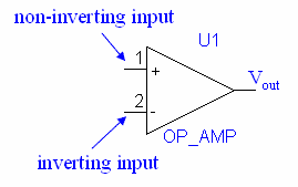
Each op-amp has an inverting input, a non-inverting input, and an output. In practice, op-amps also must be powered, but these leads are often omitted from schematics.
Ideal Op-Amps
Op-amps are generally very well described by their ideal model. There are several basic rules for ideal op-amps:
1. The output voltage satisfies , where and are the voltages at the noninverting and inverting inputs, respectively. is typically very large, such that we can consider it to be infinite. In practice, the output voltage cannot go beyond the power supply rails.
A consequence of this is that if there is any connection from the output to the inverting input, the op-amp will do its best to keep the voltages at the two inputs equal. This is called negative feedback. (Note that the op-amp won't track voltages if you connect the output back to the positive input).
2. The input current draw is zero—no current can flow in or out of the input terminals. In practice, the input impedance is on the order of to ohms.
3. The output impedance is zero. This means that there is no limit on the current the op-amp can source or sink. In practice, read the specs to find the limit.
Real Op-Amps
Here are some of the more important differences between ideal and real op-amps. These characteristics for an op-amp can usually be found in the data sheets from the manufacturer. Explantions for the terms in the spec sheets can be found at National Semiconductor's Knowledge Base
Input Offset Voltage: In a real op-amp, there will be a slight voltage difference between the inputs. This voltage difference can change with temperature.
Input Bias Current: This is the average current that flows through the two inputs.
Saturation: The output voltage is bounded by the positive and negative power supplies, known as rails. In fact, many op-amps will only go up to a few volts short of rails. If we look at the Output Voltage Swing in the data sheet for the LM411, we see that under a ±15V power source, the output will will generally be able to swing between ±13.5V—but you just might get a chip that can only output ±12V. Op-amps that are designed to be able to output voltages very close thier rails are refered to as being rail to rail.
Slew Rate: The output voltage cannot change instantaneously; the maxiumum rate of change possible for the output voltage is known as the slew rate.
Rise Time: The rise time of an op-amp is the time it takes for the output voltage to go from 10% to 90% of its final value, under a certain set of specified conditions set by the manufacturer.
Common Mode Gain: The common-mode voltage is the DC voltage shared by both pins(since they try to be the same). Ideally, the output voltage of the op-amp should only depend on the voltage difference between the inputs, but real op-amps don't have such pefectly linear gains. The effect that the common-mode voltage has on the gain is known as the common-mode gain.
The 741 and 411 Type Op-Amps
The 741 (bipolar) and 411 (FET) families of op-amps are popular chips made by many manufacturers. The model number is often preceded by a modifier/identifier, such as "LM741" or "LF411". These op-amps also come in varieties where you get multiple op-amps on a single package.
Click here for the data sheet of the LM741
[Click here for the data sheet of the LM148 quad 741]
[Click here for the data sheet of the LF411]
For now, we can ignore the "offset" pins. These are used to make very fine adjustments in the reference voltages.
For more information on how to read the op-amp data sheets, try going to National Semiconductor's Knowledge Base
Op-Amp Applications
Comparator
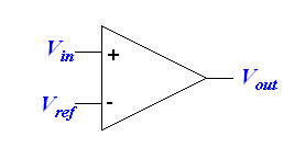
Because of its huge gain, the op-amp is very sensitive to voltage differences between its inputs. A few millivolts are enough to saturate it either way. We take advantage of this property to make a voltage comparator, which will output either a high or low depending on the input.
Voltage Follower
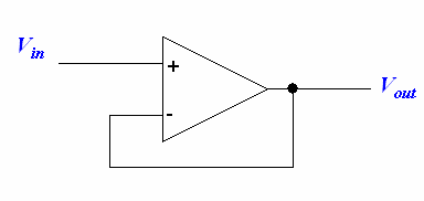
The voltage follower doesn't amplify the voltage because the output is connected back to the inverting input. However, it can be used as a buffer to isolate circuits or be used as a current amplifier.
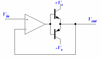
Combining the voltage follower with the push-pull follower, we get the benefits of both: zero crossover distortion (due to the op amp) and large output currents (due to the push-pull transistors).
Inverting Amplifier
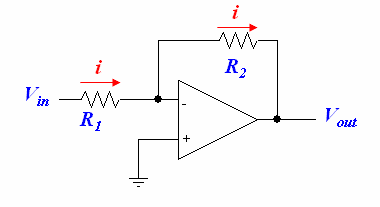
In the amplifier circuit above, we use feedback to regulate our gain. The result is an amplifier that will invert the input signal and apply a gain to it.
Since the non-inverting input is grounded and there is negative feedback, the voltage at the inverting input is also at 0V, so:
Since the op-amp inputs cannot draw current, all the current will go through and to get to . This enables us to write:
and
Combining these equations to eliminate i gives us
We now choose and ; their ratios will specify our gain. We typically choose values between 1k and 100k—if our resistances are too small, the circuit will waste power; if our resistances are too large, the tiny bit of current leaking through the op-amp may start to become noticeable.
Non-Inverting Amplifier
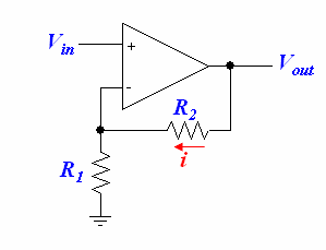
This amplifier is similar to the inverting amplifier, except it will not invert the signal. We calculate the gain as follows:
Substituting the first equation into the second yields:
Summer
Summer With Gain
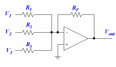
This summer circuit will output the inverted sum of the input voltages, after applying gains to the inputs. A good choice for the resistors would be about 10kΩ.
Our equations:
Summer Without Gain
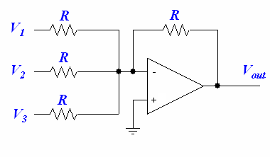
If we do not want the summer to apply any gain to the inputs, simply choose all the resistor values to be the same.
This summer circuit will output the inverted sum of the input voltages. A good choice for R would be about 10kΩ.
Question: How could you build a simple digital-to-analog converter by using different input resistances?
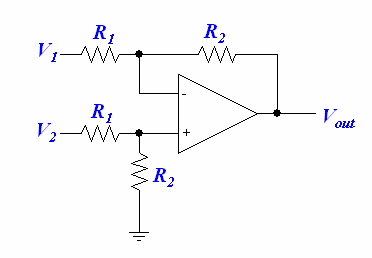
Differential Amplifier
This circuit will amplify the voltage difference between V2 and V1.
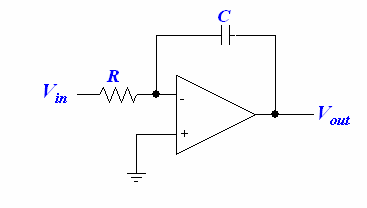
Integrator
We can build a circuit that will integrate voltage:
The output signal is a scaled and inverted integral of the input signal:
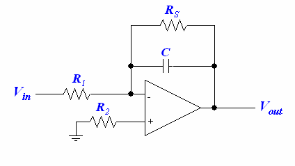
There is a problem with this circuit though—the integrator is only good if the is less than the maximum output voltage of the op-amp. Our integrator is thus not very useful for low frequency signals, becuase the charge will store up on the capacitor and eventually saturate the op-amp. Even if we have a high frequency signal, any DC offset will add up in the capacitor over time. We can remedy this problem by adding a shunt resistor across the capacitor to bleed off any long-term charges that store up in the capacitor. As a rule of thumb, should be greater than 10.
Input bias current flowing through and can generate a small DC offset, and we can try to cancel it out by adding another resistor between the non-inverting input and the ground such that
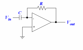
Differentiator
The differentiator will scale and invert the derivative of the input signal:
Controllers
References
Hayt, William H. Jr., Jack E. Kemmerly, and Steven M. Durbin. Engineering Circuit Analysis. 6th ed. New York:McGraw-Hill, 2002.
