Difference between revisions of "PIC16F684 Registers"
| Line 62: | Line 62: | ||
* ADC voltage reference selection (ADCON0) |
* ADC voltage reference selection (ADCON0) |
||
* ADC conversion clock source (ADCON1) |
* ADC conversion clock source (ADCON1) |
||
* Interrupt control |
* Interrupt control (INTCON) |
||
* Results formatting (ADCON0) |
* Results formatting (ADCON0) |
||
Revision as of 17:52, 10 July 2006
This page is a more detailed overview of the registers. It includes the most commonly used registers. All remaining information can be found on the Microchip website.
Memory Map
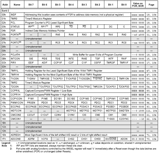
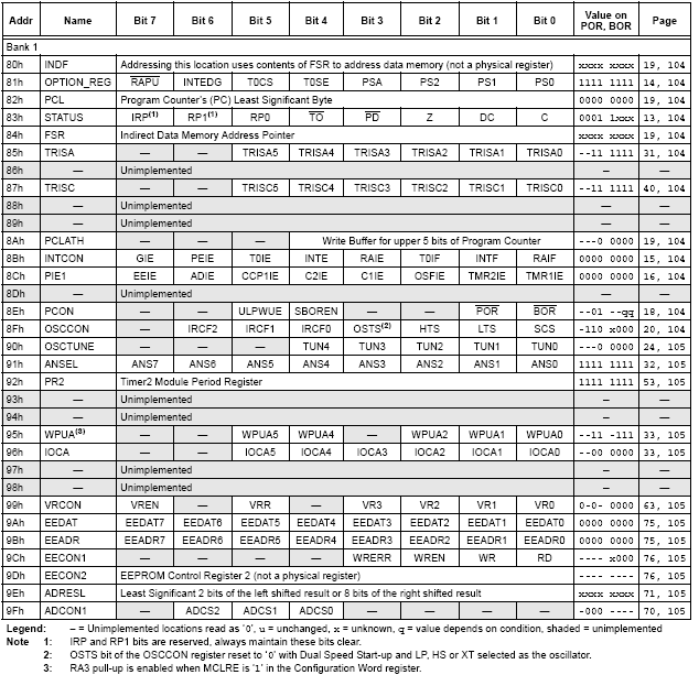
These images show the memory map of the PIC16F684. Use these for a quick reference for register addresses and initial values.
Registers in Memory Bank 0
Registers in Memory Bank 1
Register Descriptions
Configuration
STATUS
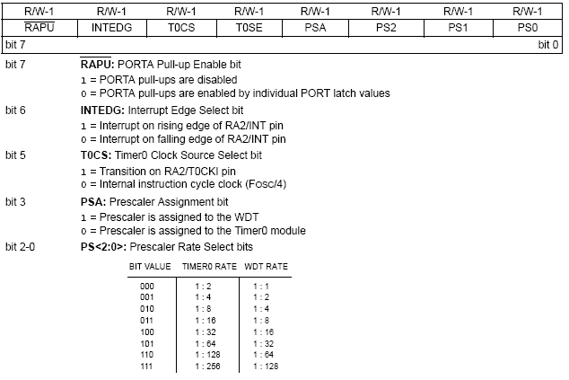
OPTION
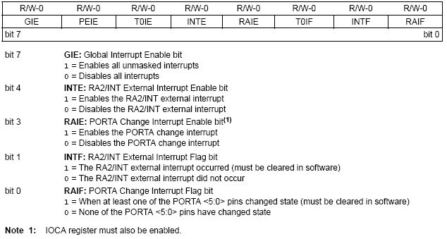
INTCON
PIE1
The PIE1 is used to enable/disable interrupts.
I/O
PORTA
TRISA
ANSEL
The ANSEL register determines whether a pin, AN<7:0>, is an analog input or not.
IOCA
The IOCA register determines whether or not an interrupt is generated when a digital pin on PORTA, RA<5:0>, experiences a change in value.
PORTC
TRISC
Timers
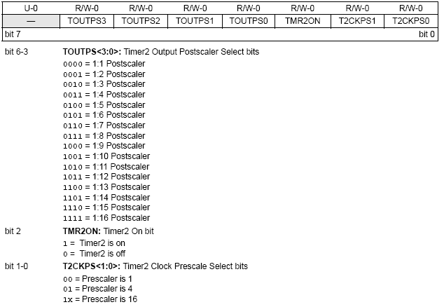
T2CON
T2CON sets up Timer2, which is used for PWM timing.
A/D Configuration and Usage
When configuring and using the ADC the following functions must be considered:
- Port configuration (ANSEL)
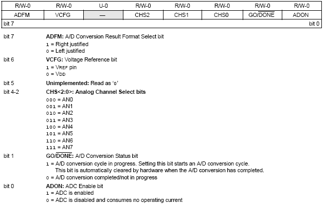
- Channel selection (ADCON0)
- ADC voltage reference selection (ADCON0)
- ADC conversion clock source (ADCON1)
- Interrupt control (INTCON)
- Results formatting (ADCON0)
ADCON1
ADCON0
ADRESH
ADRESH contains the highest significant digits of the A/D conversion. The values contained in this register depend on whether you select "Right Justified" (ADFM=1) or "Left Justified" (ADFM=0) results.
- Right Justified (ADFM=1):
- Left Justified (ADMF=0):
ADRESL
ADRESL contains the lowest significant digits of the A/D conversion. The values contained in this register depend on whether you select "Right Justified" (ADFM=1) or "Left Justified" (ADFM=0) results.
- Right Justified (ADFM=1):
- Left Justified (ADMF=0):
