Difference between revisions of "PCB Artist"
NickMarchuk (talk | contribs) |
NickMarchuk (talk | contribs) |
||
| Line 4: | Line 4: | ||
A printed circuit board, or PCB, is an epoxy board clad with copper sheets to make electrical connections along fixed routes. A PCB can have many layers of copper and insulator, depending on the complexity of the design. Layers are connected with vias, plated holes maintaining electrical conductivity. A finished PCB is often covered with solder mask, a solder-phobic layer that helps prevent solder bridges, making the PCB green. A white silk screen can be drawn on top of this, used to label the outlines of components and give other critical information. For more information on PCBs, see the wikipedia page [http://en.wikipedia.org/wiki/Printed_circuit_board Printed Circuit Board]. |
A printed circuit board, or PCB, is an epoxy board clad with copper sheets to make electrical connections along fixed routes. A PCB can have many layers of copper and insulator, depending on the complexity of the design. Layers are connected with vias, plated holes maintaining electrical conductivity. A finished PCB is often covered with solder mask, a solder-phobic layer that helps prevent solder bridges, making the PCB green. A white silk screen can be drawn on top of this, used to label the outlines of components and give other critical information. For more information on PCBs, see the wikipedia page [http://en.wikipedia.org/wiki/Printed_circuit_board Printed Circuit Board]. |
||
PCBs are created in a variety of ways. A common method is covering the copper you wish to keep and dipping the board in acid, which etches the copper you do not want. This method can be done by hand. |
PCBs are created in a variety of ways. A common method is covering the copper you wish to keep and dipping the board in acid, which etches away the copper you do not want. This method can be done by hand. |
||
A more professional and reliable PCB can be made by |
A more professional and reliable PCB can be made by designing your circuit in CAD software and ordering the part from a PCB production house. The remainder of this page will describe how to use the proprietary software PCB Artist to design and order a complete PCB. |
||
== Advanced Circuits and PCB Artist == |
== Advanced Circuits and PCB Artist == |
||
| Line 12: | Line 12: | ||
Advanced Circuits [http://www.4pcb.com (www.4pcb.com)] is a company based in Colorado known for their quick turn-around and good prices on low volume printed circuit board (PCB) orders. This is the main supplier for PCBs created by students for clasess or research at Northwestern. |
Advanced Circuits [http://www.4pcb.com (www.4pcb.com)] is a company based in Colorado known for their quick turn-around and good prices on low volume printed circuit board (PCB) orders. This is the main supplier for PCBs created by students for clasess or research at Northwestern. |
||
Previously, the PCB was created in TraxxMaker or other CAD PCB program, many of which are outdated and difficult to use, then uploaded to Advanced Circuits. Advanced Circuits has created PCB Artist, free software to create schematics and PCBs. This software is designed to order only from Advanced Circuits |
Previously, the PCB was created in TraxxMaker or other CAD PCB program, many of which are outdated and difficult to use, then uploaded to Advanced Circuits. Advanced Circuits has created PCB Artist, free software to create schematics and PCBs. This software is designed to order only from Advanced Circuits. This somewhat simplistic software is very intuitive (once comfortable) and allows for simple changes and editing. Additionally, the component library offered is up to date and contains many specific components. This Wiki page will cover the development and ordering process of a simple PCB board. |
||
====Contact at Advanced Circuits==== |
====Contact at Advanced Circuits==== |
||
Revision as of 16:26, 28 December 2009
What is a PCB?
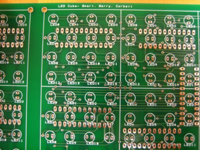
A printed circuit board, or PCB, is an epoxy board clad with copper sheets to make electrical connections along fixed routes. A PCB can have many layers of copper and insulator, depending on the complexity of the design. Layers are connected with vias, plated holes maintaining electrical conductivity. A finished PCB is often covered with solder mask, a solder-phobic layer that helps prevent solder bridges, making the PCB green. A white silk screen can be drawn on top of this, used to label the outlines of components and give other critical information. For more information on PCBs, see the wikipedia page Printed Circuit Board.
PCBs are created in a variety of ways. A common method is covering the copper you wish to keep and dipping the board in acid, which etches away the copper you do not want. This method can be done by hand.
A more professional and reliable PCB can be made by designing your circuit in CAD software and ordering the part from a PCB production house. The remainder of this page will describe how to use the proprietary software PCB Artist to design and order a complete PCB.
Advanced Circuits and PCB Artist
Advanced Circuits (www.4pcb.com) is a company based in Colorado known for their quick turn-around and good prices on low volume printed circuit board (PCB) orders. This is the main supplier for PCBs created by students for clasess or research at Northwestern.
Previously, the PCB was created in TraxxMaker or other CAD PCB program, many of which are outdated and difficult to use, then uploaded to Advanced Circuits. Advanced Circuits has created PCB Artist, free software to create schematics and PCBs. This software is designed to order only from Advanced Circuits. This somewhat simplistic software is very intuitive (once comfortable) and allows for simple changes and editing. Additionally, the component library offered is up to date and contains many specific components. This Wiki page will cover the development and ordering process of a simple PCB board.
Contact at Advanced Circuits
Jackie Sartin - Regional Sales Manager
E-mail: jackies@4pcb.com Call: 1-800-979-4PCB (4722) Ext: 1685
Getting Setup
- Have a complete circuit schematic and know exactly what parts (including part numbers) you are using.
- Download the software Or, type “PCB Artist” into google. Then click the download button in the middle of the screen.
Creating the Board
Getting Started
To start a new PCB design follow these steps:
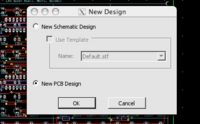
File -> New, then select "New PCB Design"
The Wizard will open, selections in the wizard
- Specify size: (mil = 1/1000 of an inch) Note: The size of the board can be changed later, this is just to get started.
- Design Requirement: For most projects you will want a "Basic" 2-layer standard. More complex boards are significantly more expensive.
- Layers: If you have selected 2-layer standard, there are few options on this page, if you have more layers you can select power and ground planes.
- Board parameters: The default selection is fine for most projects
- The next few pages are about production- click next, this will be set up later. (Ignore all cost estimates- these drastically change later)
- Name your file and save it
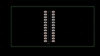
You should have a board outline on your screen. You can select which layers you view using the interaction bar on the left. (If it isn't open go file>interaction bar, or press F9)
Placing components
PCB Artist has a large libary of componets. From the screen with your board outline to add components you can do many things:
- Click the icon with the DIP in the top left of the scree
- Press F8
- Add > Component
- Click "Add Component" at the bottom of the interaction bar
Selecting your component
At this point it is important to know exactly what component you are using. This includes the exact package dimensions found on the data sheet.
Open the "Add Component" window and make sure that the "Preview" box is checked. As you scroll through the component list, a preview of the part will be displayed. This also allows you to scroll quickly looking for the appropriate part.
Note: For many parts there are multiple package options, you can select this from the package drop down menu.
- If you are using an IC it is a good idea to see if they have the exact chip. You can do this by clicking find in the "add component" window and entering the part number. This search is very hard to use. If you know the manufacturer, select it under the libraries tab and scroll to see if your component is there.
- If you are using a basic SIP or DIP package find the "PCB" library, this has many selections for SIP and DIP components. Check the package type. An N, ie DIPN, indicates narrow packaging (300mil size, vs 600mil size)
- For other components, check to see if there is a designated library, ie "diode"
- If you are using a discrete component (resistor, capacitor etc) click the Discrete library, then look through the list.
Once you have found your component click "Add." The window will close and you can now place the part by clicking. To rotate the part, just press R. To flip the part (mirror image, for the back of the PCB) press F. (When you are done with the component you can either right click or press escape.)
Once you have placed the component, measure it!!! Click the ruler icon on the lower left then click parts of the component to measure the distance between centers etc. Double check this with your part!
If you need to make a component
If you cannot find the necessary component you can build your own component. There are a couple of ways to do this:
- Add pads (add pad icon on the left - looks like a yellow doughnut) and then add outlines (the add shape icons on the middle left)
- Click libraries (Blue book on the top bar) and then create your own part using the wizard. If you do this, please add directions here.
General Building Notes
- Changing properties of the compnents, pads and connections: Right click and select properties
- To change many things at once: Click the Abc in the menu bar, top, this will open a chart with the current pads, components and sizes. To change something, click and change a value.
- Grouping functions have not been found, however you can drag select to select multiple items.
- Through the Abc button (Design Technology Window) it is possible to change many aspects of your board, check here first!
- Adding Text, this will show up on silkscreen: Click the T on the left, then enter and place the text as you would with a component
- Use the ruler to make sure your spacing is consistent (ruler icon on the left)
- To change the size of the board, select one of the board edges, green line and drag it.
Wiring and Routing the Circuit
Have your schematic out for reference.
PCB artist is helpful because it allows you to connect two points that need to be connected, with a straight line, no routing.
- Click "Add unrouted connection" button on the left (pencil with two dots)
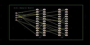
- Click the first connection point, then the second. This will leave a yellow line connecting the two points.
- Connect your entire circuit this way, it should look like yellow web.
- Go to Tools > Optimize nets to make this neater and the connections more intelligent.
Routing the Circuit
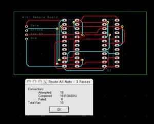
Once all of your connections are made, click the route icon on the left (blue and red wires crossing) For now stick with the default settings, you can alter these later if you need to. Click "Route." Routing will begin and a report will be generated. Routes that show up in blue are on the bottom of a 2-layer board, red is on the top.
To select an entire route, click on part of that route, then press H this will highlight the entire signal. To unroute nets: Tools> unroute nets > All nets (This will bring you back to the yellow web)
Tips on Routing
If you have a dense circuit with many signals, routing may be difficult, try the following tips. After trying any of these things, click optomize nets under tools.
- Are your components efficiently placed? Would rotating something make it more efficient? What about flipping it and putting it on the other side of the board?
- When you click the route button, in the route options window increase the effort and passes. This also increases the time it takes to route, do not max this out without changing other things too.
- Look at the desnset areas of the board (ie the center) can you move components, or rotate to free up some board space?
- Can you use a larger board?
- If you have assigned some routes to Power or Ground these are thicker by default. Unless you have a high power application, these can usually be standardized, see the Abc button.
- You can route nets by hand, much more complicated, and usually the computer is smarter, especially on complex designs.
Design Check
Once your board is routed, and before you order it, do a design check. Click the design rule check on the bottom left (2 red bars) Leave the default for basic designs. A design rule check report will be generated. If you have errors, ie pads are too small, correct them either manually by right clicking and editing or by using the Abc button at the top to change many things at once.
Ordering
Once you have a fully routed design which is error free, and has been double checked you are ready to order your board. From PCB artist you can order most options, except bare bones. To do this click order now at the very top and follow the directions. For support, call Advanced Cirucits (number at the top of the screen) or there is an ordering tutorial avalible from their website.
Ordering Options
- Barebones: These boards are very basic. They do not have solder mask (the green coating), or text on the board and the traces are exposed. However, they are fairly cheap (charged by area) and they ship in 1 business day. Perfect for prototyping. More info
- 33- Each 2 layer PCBs can be ordered for $33 each, shipping in about a week. These are complete, boards with screen printing and solder mask. The max size is 60 square inches. With the promo “student” the min qty of 4 is waived, allowing you to order a single board. More info
- Other promotions: Advanced Circuits offers various other promotions for students and first time customers. If you have questions, contact Jackie Sartin, our rep. More info
After ordering, it’s a good idea to call and make sure they have received your order, check the turn around date, promotions and any other info.
