Difference between revisions of "PCB Artist"
NickMarchuk (talk | contribs) |
Andrew Long (talk | contribs) |
||
| (64 intermediate revisions by 4 users not shown) | |||
| Line 10: | Line 10: | ||
== Advanced Circuits and PCB Artist == |
== Advanced Circuits and PCB Artist == |
||
Advanced Circuits [http://www.4pcb.com (www.4pcb.com)] is a company based in Colorado known for their quick turn-around and good prices on low volume printed circuit board (PCB) orders. This is the main supplier for PCBs created by students for |
Advanced Circuits [http://www.4pcb.com (www.4pcb.com)] is a company based in Colorado known for their quick turn-around and good prices on low volume printed circuit board (PCB) orders. This is the main supplier for PCBs created by students for clases or research at Northwestern. |
||
Previously, the PCB was created in TraxxMaker or other CAD PCB program, many of which are outdated and difficult to use, then uploaded to Advanced Circuits. Advanced Circuits has created PCB Artist, free software to create schematics and PCBs. This software is designed to order only from Advanced Circuits. This somewhat simplistic software is very intuitive (once comfortable) and allows for simple changes and editing. Additionally, the component library offered is up to date and contains many specific components. This Wiki page will cover the development and ordering process of a simple PCB board. |
Previously, the PCB was created in TraxxMaker or other CAD PCB program, many of which are outdated and difficult to use, then uploaded to Advanced Circuits. Advanced Circuits has created PCB Artist, free software to create schematics and PCBs. This software is designed to order only from Advanced Circuits. This somewhat simplistic software is very intuitive (once comfortable) and allows for simple changes and editing. Additionally, the component library offered is up to date and contains many specific components. This Wiki page will cover the development and ordering process of a simple PCB board. |
||
| Line 21: | Line 21: | ||
Call: 1-800-979-4PCB (4722) Ext: 1685 |
Call: 1-800-979-4PCB (4722) Ext: 1685 |
||
== Getting Set Up == |
|||
<br clear=all> |
|||
== Getting Setup == |
|||
*Have a complete circuit schematic and know exactly what parts (including part numbers) you are using. |
*Have a complete circuit schematic and know exactly what parts (including part numbers) you are using. |
||
| Line 52: | Line 50: | ||
*Give yourself some prototyping area and add extra vias to traces. Thus will allow you some wiggle room when your board arrives and has errors (every board will have some errors!). Traces can be cut with a razor blade fairly easily if the board is not too tight, and can be remade with wires if you remember to leave some extra vias around to solder to. |
*Give yourself some prototyping area and add extra vias to traces. Thus will allow you some wiggle room when your board arrives and has errors (every board will have some errors!). Traces can be cut with a razor blade fairly easily if the board is not too tight, and can be remade with wires if you remember to leave some extra vias around to solder to. |
||
==Download and Installation Instructions== |
|||
==Creating the Board== |
|||
Download and install PCB Artist from Advanced Circuits at [http://www.4pcb.com/index.php?load=content&page_id=46 the Advanced Artist website.] The latest version as of 1/7/2010 is 1.3.2. It is PC only and works best in Windows XP. |
|||
===Getting Started=== |
|||
[[image:Selectboard.jpg|thumb|200px|right|Selecting PCB]] |
|||
To install a library, download [[Media:ME333_Lab22.zip | the example .zip file here]]. Extract the files and place them in the PCB Artist Library folder. On Windows XP the default location is: C:\Documents and Settings\All Users\Documents\PCB Artist\Library, and on Windows Vista or Windows 7 the default location is C:\Users\Public\Documents\PCB Artist\Library. |
|||
To start a new PCB design follow these steps: |
|||
[[Image:library.jpg]] |
|||
File -> New, then select "New PCB Design" |
|||
==Create a Schematic== |
|||
The Wizard will open, selections in the wizard |
|||
Open a new schematic. |
|||
[[Image:new_schematic.jpg]] |
|||
*Specify size: (mil = 1/1000 of an inch) Note: The size of the board can be changed later, this is just to get started. |
|||
*Design Requirement: For most projects you will want a "Basic" 2-layer standard. More complex boards are significantly more expensive. |
|||
*Layers: If you have selected 2-layer standard, there are few options on this page, if you have more layers you can select power and ground planes. |
|||
*Board parameters: The default selection is fine for most projects |
|||
*The next few pages are about production- click next, this will be set up later. (Ignore all cost estimates- these drastically change later) |
|||
*Name your file and save it |
|||
Select Add a Component. |
|||
You should have a board outline on your screen. You can select which layers you view using the interaction bar on the left. (If it isn't open go file>interaction bar, or press F9) |
|||
[[Image:select_component.jpg]] |
|||
===Placing components=== |
|||
PCB Artist has a large libary of componets. From the screen with your board outline to add components you can do many things: |
|||
*Click the icon with the DIP in the top left of the screen |
|||
*Press F8 |
|||
*Add > Component |
|||
*Click "Add Component" at the bottom of the interaction bar |
|||
Choose the library your component is in (the ME333 library). |
|||
At this point it is important to know exactly what component you are using. This includes the exact package dimensions found on the data sheet. |
|||
[[Image:select_schematic_library.jpg]] |
|||
Open the "Add Component" window and make sure that the "Preview" box is checked. As you scroll through the component list, a preview of the part will be displayed. This also allows you to scroll quickly looking for the appropriate part. |
|||
Place the component R-3. Components should be arranged so that the schematic can be read and understood easily, they do not need to be laid out as they would on the PCB, we will do that later. To drag components around in the schematic, click the arrow button in the toolbar at the top to get the arrow cursor. |
|||
Note: For many parts there are multiple package options, you can select this from the package drop down menu. |
|||
[[Image:place_schematic_component.jpg]] |
|||
*If you are using an IC it is a good idea to see if they have the exact chip. You can do this by clicking find in the "add component" window and entering the part number. This search is very hard to use. If you know the manufacturer, select it under the libraries tab and scroll to see if your component is there. |
|||
*If you are using a basic SIP or DIP package find the "PCB" library, this has many selections for SIP and DIP components. Check the package type. An N, ie DIPN, indicates narrow packaging (300mil size, vs 600mil size) |
|||
*For other components, check to see if there is a designated library, ie "diode" |
|||
*If you are using a discrete component (resistor, capacitor etc) click the Discrete library, then look through the list. |
|||
Add the LED from the ME333 library and connect the components using the Add Schematic Connection tool (the icon on the left that looks like a pencil drawing a line). Such connections will make it easier to create the PCB. They indicate which pins need to be connected on the PCB, but they do not represent the actual paths the traces will take. We will design those later. |
|||
[[image:DropComp.jpg|thumb|200px|right|Adding Component]] |
|||
[[Image:connect_schematic_components.jpg]] |
|||
Once you have found your component click "Add." The window will close and you can now place the part by clicking. To rotate the part, just press R. To flip the part (mirror image, for the back of the PCB) press F. (When you are done with the component you can either right click or press escape.) |
|||
Add a voltage source and ground from the Schema library and connect them to the schematic. |
|||
Once you have placed the component, measure it!!! Click the ruler icon on the lower left then click parts of the component to measure the distance between centers etc. Double check this with your part! |
|||
[[Image:complete_schematic.jpg]] |
|||
====If you need to make a component==== |
|||
If you cannot find the necessary component you can build your own component. There are a couple of ways to do this: |
|||
*Add pads (add pad icon on the left - looks like a yellow doughnut) and then add outlines (the add shape icons on the middle left) |
|||
*Click libraries (Blue book on the top bar) and then create your own part using the wizard. If you do this, please add directions here. |
|||
Save the file (.sch). Now we can design a PCB for this circuit. |
|||
=== General Building Notes=== |
|||
*Changing properties of the compnents, pads and connections: Right click and select properties |
|||
*To change many things at once: Click the Abc in the menu bar, top, this will open a chart with the current pads, components and sizes. To change something, click and change a value. |
|||
* Grouping functions have not been found, however you can drag select to select multiple items. |
|||
*Through the Abc button (Design Technology Window) it is possible to change many aspects of your board, check here first! |
|||
*Adding Text, this will show up on silkscreen: Click the T on the left, then enter and place the text as you would with a component |
|||
*Use the ruler to make sure your spacing is consistent (ruler icon on the left) |
|||
*To change the size of the board, select one of the board edges, green line and drag it. |
|||
==Create PCB from Schematic== |
|||
===Wiring and Routing the Circuit=== |
|||
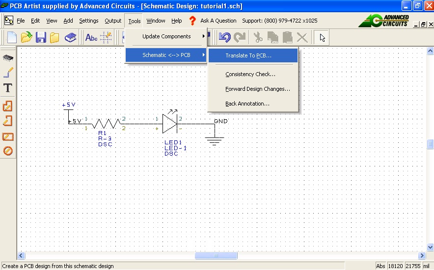
Open your schematic and go to Tools, Schematic <--> PCB, Translate to PCB. |
|||
[[image:netweb.jpg|thumb|300px|right|Nets Connecting Pads, A yellow web]] |
|||
[[Image:translate_to_pcb.jpg]] |
|||
Have your schematic out for reference. |
|||
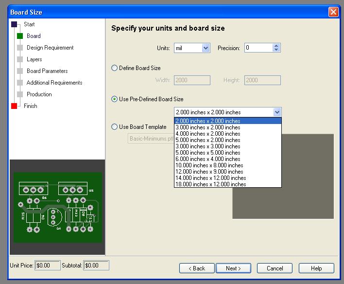
Go through the New PCB Wizard, selecting your board size or defining a custom size. This can always be changed later if you need a larger or smaller board. |
|||
PCB artist is helpful because it allows you to connect two points that need to be connected, with a straight line, no routing. |
|||
[[Image:board_size.jpg]] |
|||
*Click "Add unrouted connection" button on the left (pencil with two dots) |
|||
*Click the first connection point, then the second. This will leave a yellow line connecting the two points. |
|||
*Connect your entire circuit this way, it should look like yellow web. |
|||
*Go to Tools > Optimize nets to make this neater and the connections more intelligent. |
|||
Use a 2 layer board with the default properties. At this screen, |
|||
====Routing the Circuit==== |
|||
[[image:routedcircuit.jpg|thumb|300px|right|A routed circuit]] |
|||
[[Image:special_reqs.jpg]] |
|||
Once all of your connections are made, click the route icon on the left (blue and red wires crossing) |
|||
For now stick with the default settings, you can alter these later if you need to. |
|||
Click "Route." Routing will begin and a report will be generated. |
|||
Routes that show up in blue are on the bottom of a 2-layer board, red is on the top. |
|||
do not enter anything, but later we will add a comment to allow us to buy a Student discount board for $33 plus shipping. |
|||
To select an entire route, click on part of that route, then press H this will highlight the entire signal. |
|||
To unroute nets: Tools> unroute nets > All nets (This will bring you back to the yellow web) |
|||
Enter a board number and revision number. Use a 1 week turn around with 1 unit. Ignore the cost, that will change to $33 later. |
|||
====Tips on Routing==== |
|||
If you have a dense circuit with many signals, routing may be difficult, try the following tips. After trying any of these things, click optomize nets under tools. |
|||
*Are your components efficiently placed? Would rotating something make it more efficient? What about flipping it and putting it on the other side of the board? |
|||
*When you click the route button, in the route options window increase the effort and passes. This also increases the time it takes to route, do not max this out without changing other things too. |
|||
*Look at the desnset areas of the board (ie the center) can you move components, or rotate to free up some board space? |
|||
*Can you use a larger board? |
|||
*If you have assigned some routes to Power or Ground these are thicker by default. Unless you have a high power application, these can usually be standardized, see the Abc button. |
|||
*You can route nets by hand, much more complicated, and usually the computer is smarter, especially on complex designs. |
|||
[[Image:pcb_production.jpg]] |
|||
===Design Check=== |
|||
Once your board is routed, and before you order it, do a design check. |
|||
Click the design rule check on the bottom left (2 red bars) |
|||
Leave the default for basic designs. A design rule check report will be generated. If you have errors, ie pads are too small, correct them either manually by right clicking and editing or by using the Abc button at the top to change many things at once. |
|||
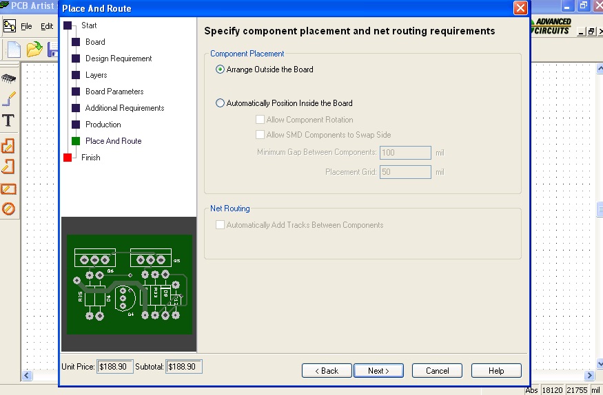
Have the program place the components outside of your board so you can arrange them where you want them. |
|||
== Ordering == |
|||
Once you have a fully routed design which is error free, and has been double checked you are ready to order your board. |
|||
From PCB artist you can order most options, except bare bones. To do this click order now at the very top and follow the directions. For support, call Advanced Cirucits (number at the top of the screen) or there is an ordering tutorial avalible from [http://www.4pbc.com their website]. |
|||
[[Image:place_components.jpg]] |
|||
===Ordering Options=== |
|||
*Barebones: These boards are very basic. They do not have solder mask (the green coating), or text on the board and the traces are exposed. However, they are fairly cheap (charged by area) and they ship in 1 business day. Perfect for prototyping. [http://www.barebonespcb.com More info] |
|||
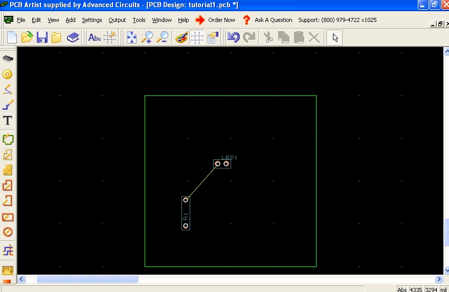
Translate the components to the inside of the green box which represents the outline of your board. Rotate a component by right clicking on the part and choosing rotate. All of the components must be moved inside of the green box to finish the board. These will be their locations on the board. |
|||
[[Image:move_and_rotate.jpg]] |
|||
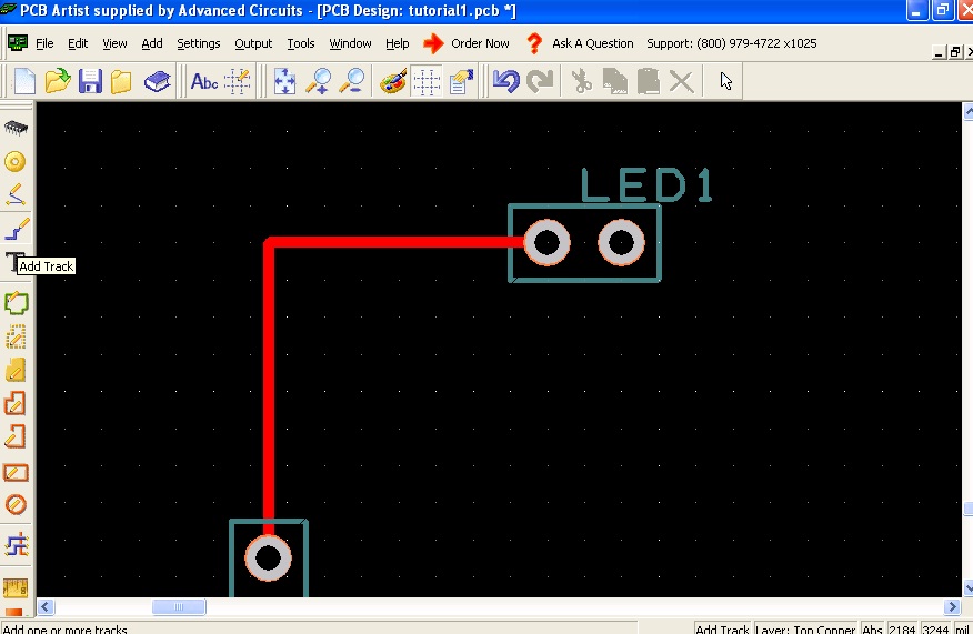
Select Add Track and connect the pins connected by the yellow line. Try to follow a convention, like a grid, to make things easier on more complicated boards. The default track width should be fine for most purposes. If there will be a lot of current flowing on the track, you should make it wider by right-clicking and choosing Properties. Tracks can be as wide as you want, within the spacing constraints. Ground tracks are often chosen to be as wide as possible. |
|||
[[Image:add_trace.jpg]] |
|||
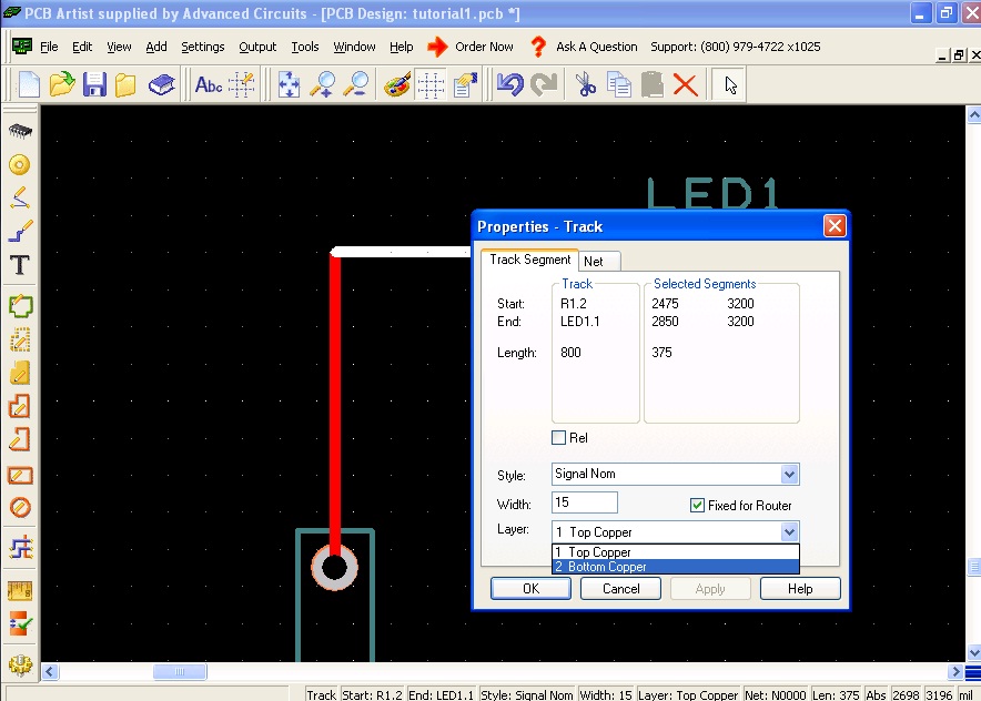
A good convention is to have traces running vertically be on one side of the board, and traces running horizontally be on the other. Select a portion of the trace, right click and select Properties. Here you can change the layer of the board and the width of the trace. |
|||
[[Image:edit_trace.jpg]] |
|||
Notice how the traces are automatically connected with a via to maintain connection. |
|||
[[Image:automatic_via.jpg]] |
|||
Traces do not have to be drawn orthogonally. While drawing a trace, right click and select segment mode. These different modes will draw traces in a different way. Miter is the most common. |
|||
[[Image:miter_trace.jpg]] |
|||
An orthogonally drawn trace can be turned into a miter by double clicking the corner and dragging the corner in. |
|||
Use the Add Pad button and Add track to complete the circuit. You need to add these vias to make the power and ground connections because they do not translate from the Schematic Schema to the PCB. If you were to make this board, you would solder wires to these vias to supply power. |
|||
[[Image:add_via.jpg]] |
|||
Add some text reminders to the silkscreen layer to remind yourself where to solder the power and ground, what direction the LED goes, and what resistor to use. |
|||
[[Image:add_text.jpg]] |
|||
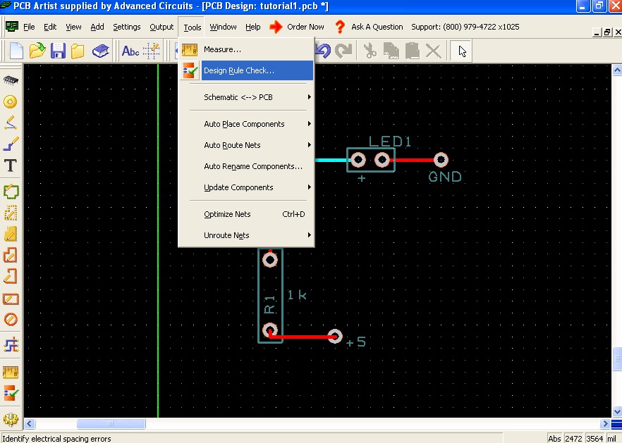
When your board is complete, use the Design Rule Check to automatically look for errors in connecting pins and accidentally crossed traces. You can check all the boxes. |
|||
[[Image:design_rule_check.jpg]] |
|||
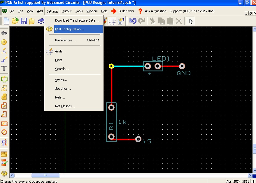
Go to Settings, PCB Configuration to make your board bigger or smaller or change other properties. You can also click on specific edges of your board to resize the board, or use the arrow to drag a box around all the components to select them and drag them around inside the board. |
|||
[[Image:pcb_config.jpg]] |
|||
Use this document, [[Media:Student Order Process updated 4-14.pdf|Student Order Process]], to purchase a board with the $33 Student Discount. (Maximum board size for this special is 60 square inches.) |
|||
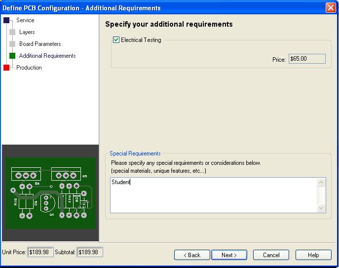
Go back to PCB Configuration and Enter Student in the Special Requirements section. |
|||
[[Image:student_order.jpg]] |
|||
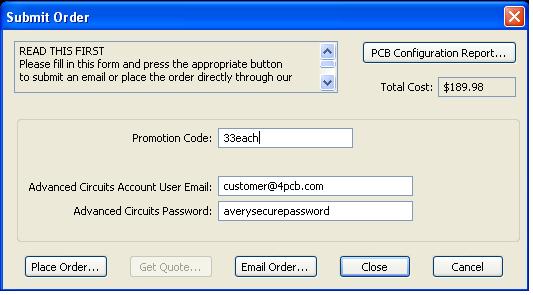
Go to Output, Submit Order. PCB Artist will perform a Design Rule Check. After that, enter the Promotion Code 33each. If you do not have an Advanced Circuits account, go to [http://www.4pcb.com 4pcb.com] and make one. Then you may order your board. |
|||
[[Image:submit_order.jpg]] |
|||
==Adding a Component to the Library== |
|||
A majority of the time the component you want to use is not in the existing libraries, therefore, you have to create a component. A component consists of a schematic symbol, a pcb symbol and a mapping between the pins of the schematic symbol and the pcb symbol. This section details how to create a component using the SN74HC04 Hex Inverter as an example. |
|||
===Create a Schematic Symbol=== |
|||
With PCBArtist open (it doesn't matter if any schematics or pcb files are open), click on the blue book at the top of the screen. |
|||
[[Image:PCBArtist_BlueBook.jpg]] |
|||
<br clear=all> |
|||
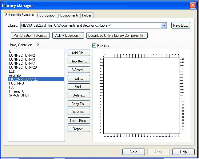
This opens the Library Manager of schematic symbols, pcb symbols and components. It will look something similar to the image below. |
|||
[[Image:PCBArtist_LibraryManager.jpg]] |
|||
<br clear=all> |
|||
To make a component, we first need to download the datasheet of the component. Download the datasheet for the Hex Inverter [[Media:SN74HC04Inverter.pdf|here]]. |
|||
<br clear=all> |
|||
On the first page of the datasheet, we can find a schematic of the component for SN74HC04. We will use this schematic to make our schematic in PCB Artist. |
|||
*In PCBArtist, click on the 'Schematic Tab' of the Library Manager. |
|||
*Click on the 'Wizard' Button in the middle of the window to begin creating a schematic symbol. |
|||
This wizard will help you make your schematic symbols. |
|||
*Click 'Next' |
|||
[[Image:PCBArtist_Sch_Start.jpg]] |
|||
<br clear=all> |
|||
*Choose English with a precision of 1 (these are the units for the symbol) |
|||
*Click 'Next' |
|||
[[Image:PCBArtist_Sch_Tech.jpg]] |
|||
<br clear=all> |
|||
*Next we are going to choose the type of symbol. Our chip has pins on two sides so select the rectangle with pins on two sides (the first one). |
|||
*Select the 'center' option for Origin. If you decide to rotate the symbol, it will rotate about this point. |
|||
*Select the top left corner for Component Name. This indicates where the component name will be placed. |
|||
*Click 'Next' |
|||
[[Image:PCBArtist_Sch_SymbolType.jpg]] |
|||
<br clear=all> |
|||
*In the next window, you can choose how you want the pins to be represented, the size of these and the length of the lines going to the pins. Leave these with the default values. |
|||
*Click 'Next' |
|||
[[Image:PCBArtist_Sch_Styles.jpg]] |
|||
<br clear=all> |
|||
The next window determines the number of pins on each side of the component and some dimensions. |
|||
*Enter 7 for both Pins on left and Pins on Right. |
|||
*The other dimensions are not as important for the schematic, leave these as the default. (They can be editted later if too big or too small). |
|||
*The last part on this page describes how the pins are numbered. Since the schematic on the datasheet spirals the numbers, select the 'Spiral Round' option. |
|||
*Click 'Next' |
|||
[[Image:PCBArtist_Sch_Pins.jpg]] |
|||
<br clear=all> |
|||
The last window is where you name the symbol and save it to a specific library. |
|||
*Name the component SN74HC04_Inverter and save it in the ME333_Lab2 Library that you downloaded above. |
|||
*Click Finish |
|||
You have now created a schematic symbol. If you checked the 'Edit the symbol now' box, you can see the schematic and edit if you want. We won't do any editting right now though. |
|||
[[Image:PCBArtist_Sch_Finish.jpg]] |
|||
<br clear=all> |
|||
===Create a PCB Symbol=== |
|||
The next step is to create a pcb symbol for the component. This will be the footprint on your PCB. Look at the datasheet again and find the Plastic Dual-In Line Package footprint for the SN74HC04 (page 10). This tells us the dimensions we need for our footprint. |
|||
*Click on the Library Manager (blue book). |
|||
*Go to the PCB Symbols tab. |
|||
*Click on the Wizard again. |
|||
*Click Next on the start up window. |
|||
*On the Technology window, choose English with 'thou' as the unit and precision of 1. We choose this because it is the smallest unit on the datasheet for the English units. |
|||
The next window is the footprint type. |
|||
* Select DIP type (the top left). |
|||
* For Origin - select center |
|||
* For Name - select center - this is where the name will be displayed on the PCB |
|||
*Click 'Next' |
|||
[[Image:PCBArtist_PCB_FootPrint.jpg]] |
|||
<br clear=all> |
|||
The next window describes the pads on the PCB. This window will be different for the different types of chips. |
|||
*Choose 14 pads |
|||
*For the Pad Style, choose 'Round' and leave Style blank. |
|||
The units are in thousands of inches |
|||
*e = 100 for 0.1 in pitch (as shown on the datasheet). |
|||
*E = 400. We can put this value between 325 and 430 as shown on the datasheet, but we also know that the chip can plug into a breadboard (spacings of 0.1 in), so 400 thou is a good number. |
|||
*PW = 60 and HD = 30. HD refers to the hole diameter for the pin. The pin diameter is around 20 thou as shown on the datasheet, so 30 thou is a good number with extra space. PW is the pad width (extra copper) surrounding the hole. Extra 30 thou is generally a good pad width. |
|||
*Choose Pin 1 Position to be the lower left corner (same as in the footprint on the datasheet) |
|||
*We don't want the pin numbers to be displayed on the PCB so select Hide for the Pin Numbers |
|||
*Pin number is counter clockwise. |
|||
*Click Next |
|||
[[Image:PCBArtist_PCB_Pads.jpg]] |
|||
<br clear=all> |
|||
The next window describes the silk screen (the writing on top of the PCB). |
|||
*Click Yes |
|||
*Layer - Top Silkscreen |
|||
*Inside pads by 25 (sometimes you may want the silk screen to be outside the pads, but it is really your choice) |
|||
*Include Marks - Notch at end (12.5) --> this helps you figure out the orientation of the component |
|||
*Click Next |
|||
[[Image:PCBArtist_PCB_SilkScreen.jpg]] |
|||
<br clear=all> |
|||
The next window asks if you want a placement shape (rectangle) around the entire component. We are not going to include this. |
|||
*Click No |
|||
*Click Next |
|||
*On the final window, name it SN74HC04_Inverter (same name as the schematic) and save it in the ME333 Library. |
|||
*Click Finish |
|||
You have now created a PCB footprint. |
|||
<br clear=all> |
|||
===Create a Component=== |
|||
We created a schematic symbol and a pcb symbol above. Now we are going to create a component to link the two symbols. |
|||
*Click on the Library Manager and go to the Component tab. |
|||
*Click on the Wizard button |
|||
*Click Next on the opening window |
|||
The first window allows you to select what type of component you are making. You can make a Normal Component (both Schematic and PCB), only a Schematic component or only a PCB component. |
|||
*Select Normal Component |
|||
*Click Next |
|||
This windows contains the details for the component. |
|||
*Name = SN74HC04_Inverter (same as the symbols) |
|||
*Package - type DIP (this really doesn't matter) |
|||
*Default Reference - choose IC for integrated circuit |
|||
*Component pins - 14 |
|||
*Number of Gates - 1 - this is the number of times your schematic symbol is needed for the component |
|||
*Click Next |
|||
[[Image:PCBArtist_Component_Details.jpg]] |
|||
<br clear=all> |
|||
In the next window you select the schematic symbol that you want to use |
|||
*Select SN74HC04_Inverter from the ME333 Library |
|||
*Click Next |
|||
In the PCB window, you select the pcb symbol that you want to use |
|||
*Select SN74HC04_Inverter from the ME333 Library |
|||
*Click Next |
|||
The next window assigns the pins from the schematic to the pcb. |
|||
Since we choose our pins in the schematic and pcb to have the same order: |
|||
*Select Assign 1-to-1 button to assign Pin 1 Schematic to Pin 1 PCB ... etc |
|||
We can also choose to add names to each pin. |
|||
*Assign the pins names (1A,1Y,GND..etc) to each of the pins as shown on the datasheet. |
|||
*Click Next |
|||
[[Image:PCBArtist_Component_Pins.jpg]] |
|||
<br clear=all> |
|||
On the final window: |
|||
*33- Each 2 layer PCBs can be ordered for $33 each, shipping in about a week. These are complete, boards with screen printing and solder mask. The max size is 60 square inches. With the promo “student” the min qty of 4 is waived, allowing you to order a single board. [http://www.4pcb.com/index.php?load=content&page_id=130 More info] |
|||
*Click Save the component to the library --> Put it in the ME333 library |
|||
If you want to edit the component now (check the next box) |
|||
*Click finish |
|||
You have now created a component and can use it with schematics and pcbs. |
|||
*Other promotions: Advanced Circuits offers various other promotions for students and first time customers. If you have questions, contact Jackie Sartin, our rep. [http://www.4pcb.com/index.php?load=content&page_id=129 More info] |
|||
== Practice Making a PCB == |
|||
After ordering, it’s a good idea to call and make sure they have received your order, check the turn around date, promotions and any other info. |
|||
After reviewing this tutorial, you are ready to [[Practice Making a PCB]]. |
|||
Latest revision as of 16:01, 13 January 2010
What is a PCB?
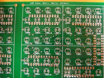
A printed circuit board, or PCB, is an epoxy board clad with copper sheets to make electrical connections along fixed routes. A PCB can have many layers of copper and insulator, depending on the complexity of the design. Layers are connected with vias, plated holes maintaining electrical conductivity. A finished PCB is often covered with solder mask, a solder-phobic layer that helps prevent solder bridges, making the PCB green. A white silk screen can be drawn on top of this, used to label the outlines of components and give other critical information. For more information on PCBs, see the wikipedia page Printed Circuit Board.
PCBs are created in a variety of ways. A common method is covering the copper you wish to keep and dipping the board in acid, which etches away the copper you do not want. This method can be done by hand.
A more professional and reliable PCB can be made by designing your circuit in CAD software and ordering the part from a PCB production house. The remainder of this page will describe how to use the proprietary software PCB Artist to design and order a complete PCB.
Advanced Circuits and PCB Artist
Advanced Circuits (www.4pcb.com) is a company based in Colorado known for their quick turn-around and good prices on low volume printed circuit board (PCB) orders. This is the main supplier for PCBs created by students for clases or research at Northwestern.
Previously, the PCB was created in TraxxMaker or other CAD PCB program, many of which are outdated and difficult to use, then uploaded to Advanced Circuits. Advanced Circuits has created PCB Artist, free software to create schematics and PCBs. This software is designed to order only from Advanced Circuits. This somewhat simplistic software is very intuitive (once comfortable) and allows for simple changes and editing. Additionally, the component library offered is up to date and contains many specific components. This Wiki page will cover the development and ordering process of a simple PCB board.
Contact at Advanced Circuits
Jackie Sartin - Regional Sales Manager
E-mail: jackies@4pcb.com Call: 1-800-979-4PCB (4722) Ext: 1685
Getting Set Up
- Have a complete circuit schematic and know exactly what parts (including part numbers) you are using.
- Download the software Or, type “PCB Artist” into google. Then click the download button in the middle of the screen.
- Review the material on this page: Help Guides and User Reference documents
Browse through the Advanced Circuits tutorial pdf to get familiar with the program interface and design process. In general, you will:
- Create a schematic (.sch) that represents the circuit you want to create. This schematic is just like any other schematic you would draw by hand, but it will be used to automate the process of laying out your physical PCB and is very helpful in debugging.
- Create a PCB design (.pcb) that represents your physical PCB, based on your schematic. In this CAD process, the program will automatically grab the components you need and place them outside of the board. You then place each component and connect the pins based on how they are connected in the schematic. The program helps you by highlighting the nets (all the pins that need to be connected) in different colors. You choose how to connect each pin, the width of the copper trace, the layer the copper should be on (top or bottom for a 2 sided board), and the size of the vias. You can have PCB Artist automatically place your components and connect them, but the result may not be pretty or successful.
- Check for errors. Use the Design Rule Check tool to make sure the board is machinable and the pins are connected as they are in your schematic. Carefully scan your board to make sure vias don't accidentally touch traces. Put some silk screen labels next to pins and components, and put your name and the version of your board somewhere for later reference.
- Order your board! Use the student deal ($33 for one board), but note it generally takes a week to make and a few days to ship (another $15). So order early and design carefully.
Some general tips:
- Don't try to make a 2" x 2" board if your space constraints allow for a larger board. It is not worth the effort and possible mistakes trying to squeeze everything into a tiny area if you don't have to.
- Connect your power and ground traces first, they are usually the most complicated.
- Try to keep an organized board. Keep components with many connections close together.
- Use a convention like top layer traces go left-right and bottom layer traces go up-down, this will make routing much easier.
- Give yourself some prototyping area and add extra vias to traces. Thus will allow you some wiggle room when your board arrives and has errors (every board will have some errors!). Traces can be cut with a razor blade fairly easily if the board is not too tight, and can be remade with wires if you remember to leave some extra vias around to solder to.
Download and Installation Instructions
Download and install PCB Artist from Advanced Circuits at the Advanced Artist website. The latest version as of 1/7/2010 is 1.3.2. It is PC only and works best in Windows XP.
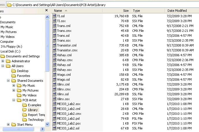
To install a library, download the example .zip file here. Extract the files and place them in the PCB Artist Library folder. On Windows XP the default location is: C:\Documents and Settings\All Users\Documents\PCB Artist\Library, and on Windows Vista or Windows 7 the default location is C:\Users\Public\Documents\PCB Artist\Library.
Create a Schematic
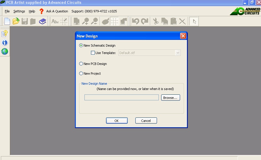
Open a new schematic.
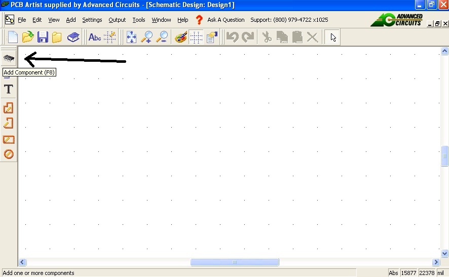
Select Add a Component.
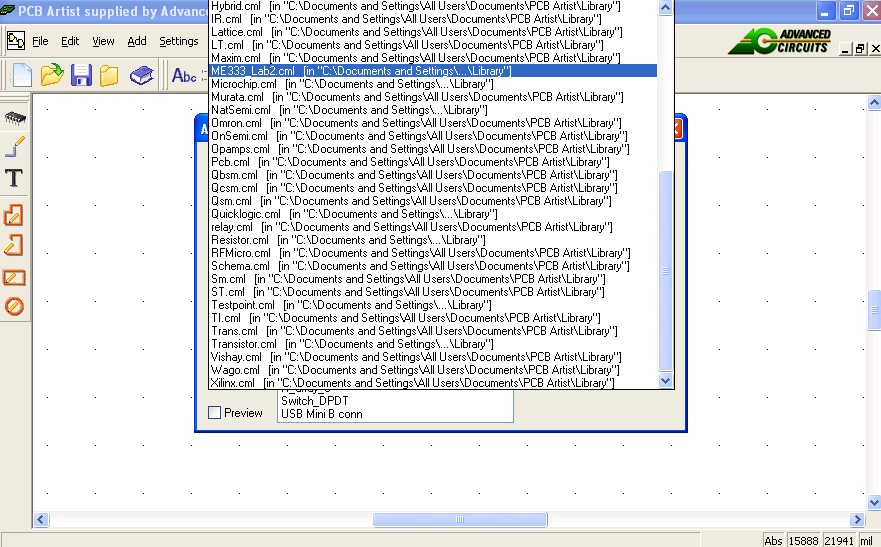
Choose the library your component is in (the ME333 library).
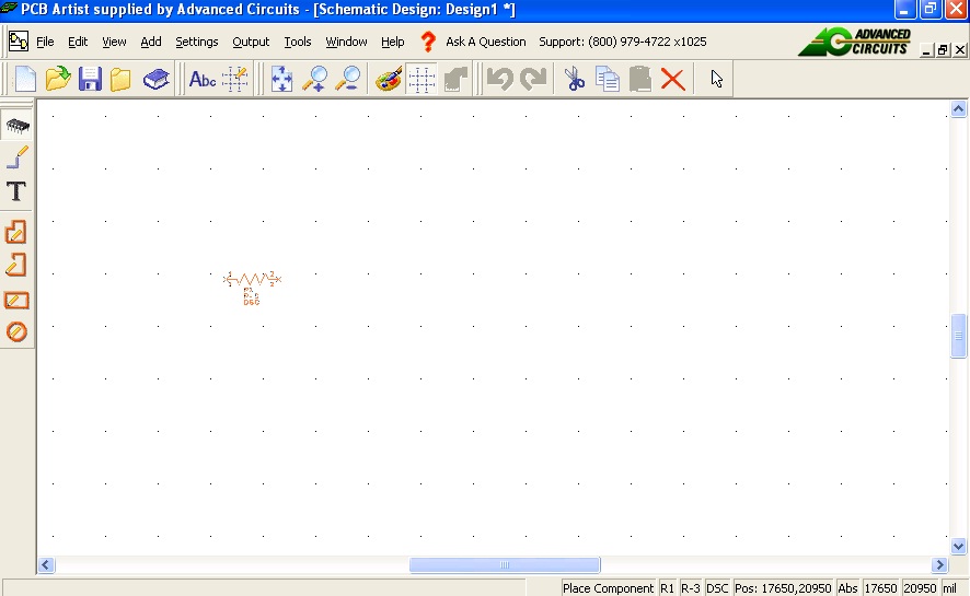
Place the component R-3. Components should be arranged so that the schematic can be read and understood easily, they do not need to be laid out as they would on the PCB, we will do that later. To drag components around in the schematic, click the arrow button in the toolbar at the top to get the arrow cursor.
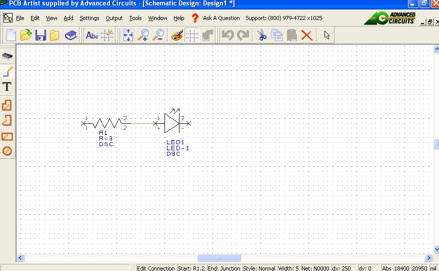
Add the LED from the ME333 library and connect the components using the Add Schematic Connection tool (the icon on the left that looks like a pencil drawing a line). Such connections will make it easier to create the PCB. They indicate which pins need to be connected on the PCB, but they do not represent the actual paths the traces will take. We will design those later.
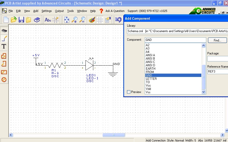
Add a voltage source and ground from the Schema library and connect them to the schematic.
Save the file (.sch). Now we can design a PCB for this circuit.
Create PCB from Schematic
Open your schematic and go to Tools, Schematic <--> PCB, Translate to PCB.
Go through the New PCB Wizard, selecting your board size or defining a custom size. This can always be changed later if you need a larger or smaller board.
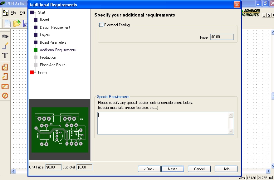
Use a 2 layer board with the default properties. At this screen,
do not enter anything, but later we will add a comment to allow us to buy a Student discount board for $33 plus shipping.
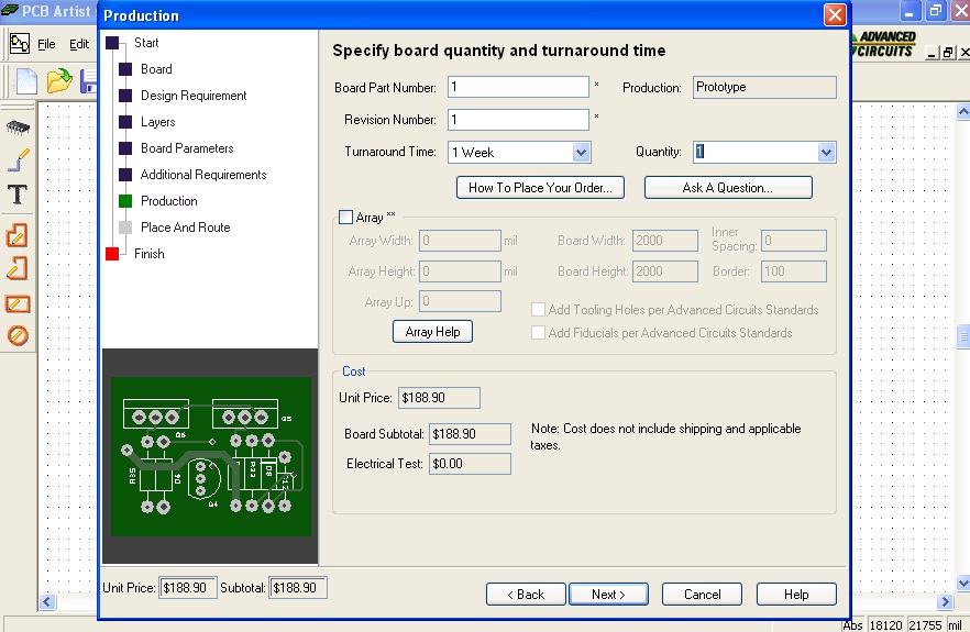
Enter a board number and revision number. Use a 1 week turn around with 1 unit. Ignore the cost, that will change to $33 later.
Have the program place the components outside of your board so you can arrange them where you want them.
Translate the components to the inside of the green box which represents the outline of your board. Rotate a component by right clicking on the part and choosing rotate. All of the components must be moved inside of the green box to finish the board. These will be their locations on the board.
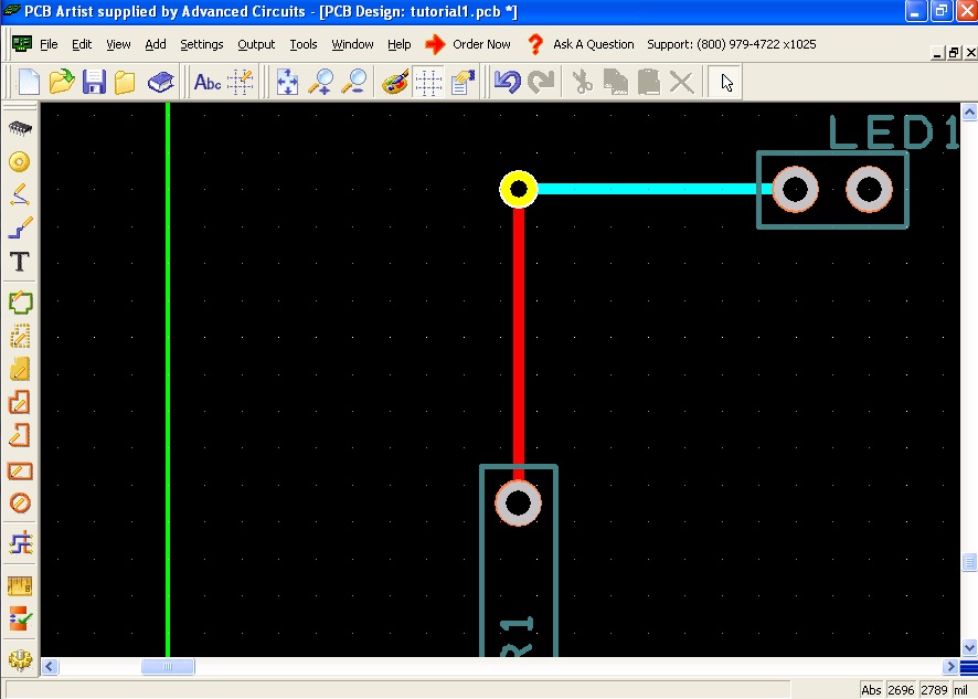
Select Add Track and connect the pins connected by the yellow line. Try to follow a convention, like a grid, to make things easier on more complicated boards. The default track width should be fine for most purposes. If there will be a lot of current flowing on the track, you should make it wider by right-clicking and choosing Properties. Tracks can be as wide as you want, within the spacing constraints. Ground tracks are often chosen to be as wide as possible.
A good convention is to have traces running vertically be on one side of the board, and traces running horizontally be on the other. Select a portion of the trace, right click and select Properties. Here you can change the layer of the board and the width of the trace.
Notice how the traces are automatically connected with a via to maintain connection.
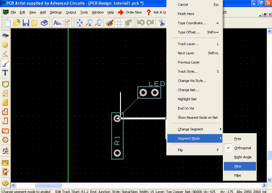
Traces do not have to be drawn orthogonally. While drawing a trace, right click and select segment mode. These different modes will draw traces in a different way. Miter is the most common.
An orthogonally drawn trace can be turned into a miter by double clicking the corner and dragging the corner in.
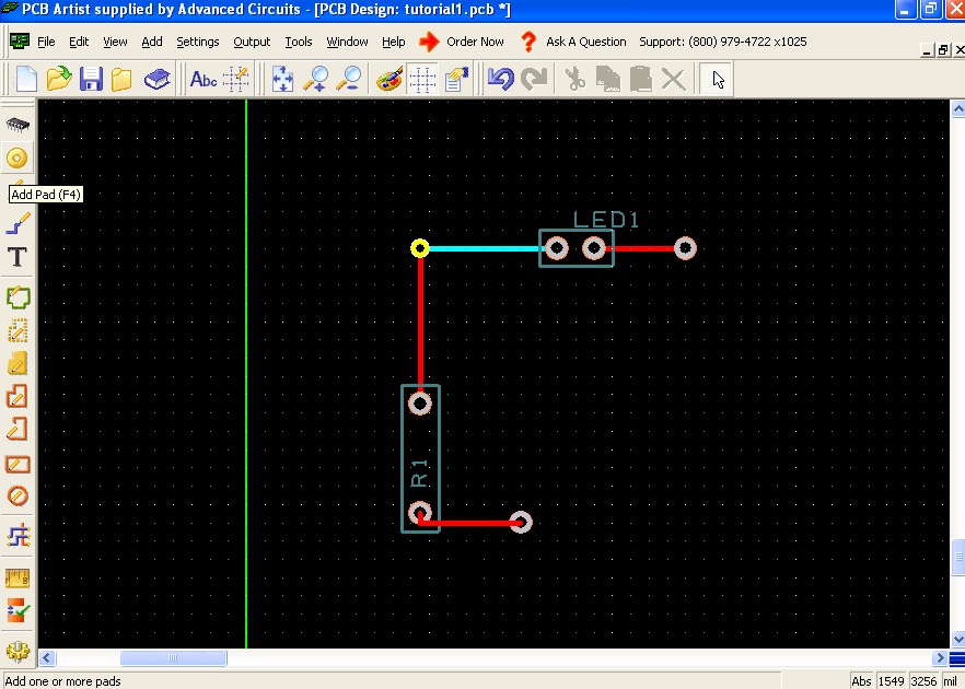
Use the Add Pad button and Add track to complete the circuit. You need to add these vias to make the power and ground connections because they do not translate from the Schematic Schema to the PCB. If you were to make this board, you would solder wires to these vias to supply power.
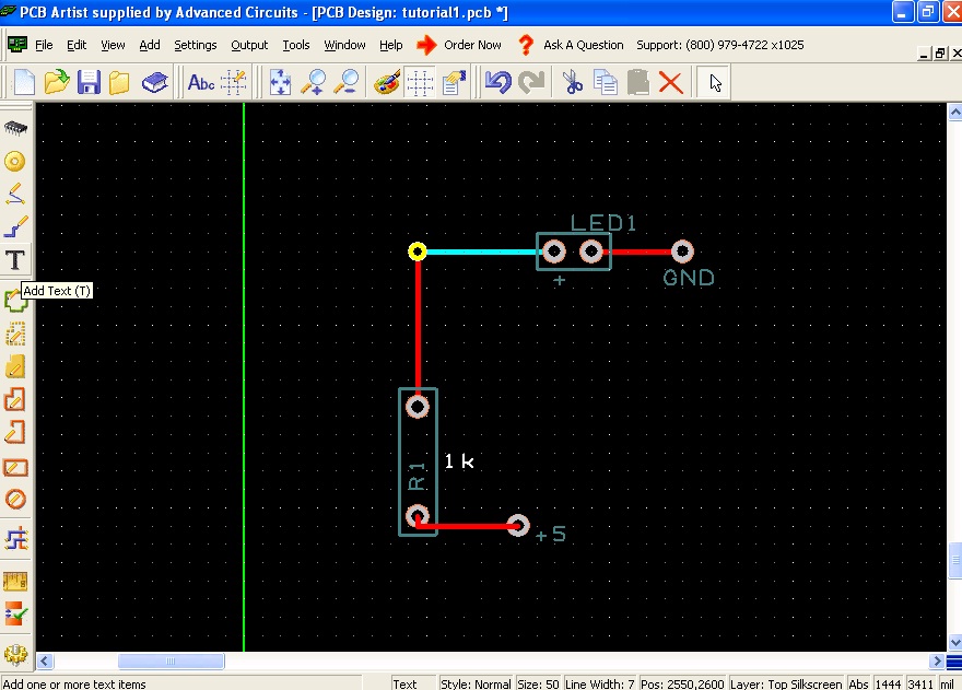
Add some text reminders to the silkscreen layer to remind yourself where to solder the power and ground, what direction the LED goes, and what resistor to use.
When your board is complete, use the Design Rule Check to automatically look for errors in connecting pins and accidentally crossed traces. You can check all the boxes.
Go to Settings, PCB Configuration to make your board bigger or smaller or change other properties. You can also click on specific edges of your board to resize the board, or use the arrow to drag a box around all the components to select them and drag them around inside the board.
Use this document, Student Order Process, to purchase a board with the $33 Student Discount. (Maximum board size for this special is 60 square inches.)
Go back to PCB Configuration and Enter Student in the Special Requirements section.
Go to Output, Submit Order. PCB Artist will perform a Design Rule Check. After that, enter the Promotion Code 33each. If you do not have an Advanced Circuits account, go to 4pcb.com and make one. Then you may order your board.
Adding a Component to the Library
A majority of the time the component you want to use is not in the existing libraries, therefore, you have to create a component. A component consists of a schematic symbol, a pcb symbol and a mapping between the pins of the schematic symbol and the pcb symbol. This section details how to create a component using the SN74HC04 Hex Inverter as an example.
Create a Schematic Symbol
With PCBArtist open (it doesn't matter if any schematics or pcb files are open), click on the blue book at the top of the screen.

This opens the Library Manager of schematic symbols, pcb symbols and components. It will look something similar to the image below.
To make a component, we first need to download the datasheet of the component. Download the datasheet for the Hex Inverter here.
On the first page of the datasheet, we can find a schematic of the component for SN74HC04. We will use this schematic to make our schematic in PCB Artist.
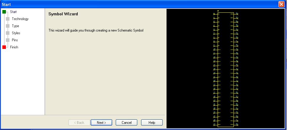
- In PCBArtist, click on the 'Schematic Tab' of the Library Manager.
- Click on the 'Wizard' Button in the middle of the window to begin creating a schematic symbol.
This wizard will help you make your schematic symbols.
- Click 'Next'
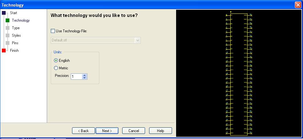
- Choose English with a precision of 1 (these are the units for the symbol)
- Click 'Next'
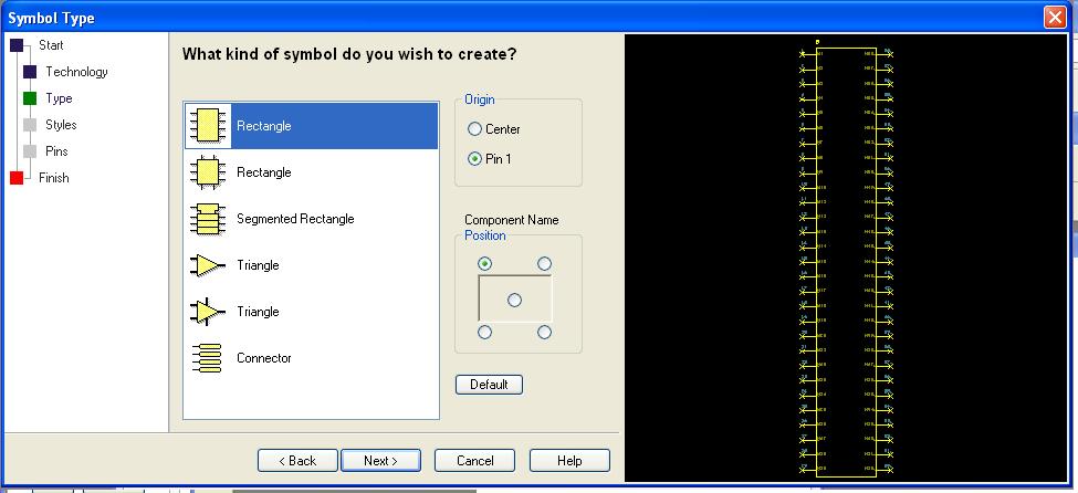
- Next we are going to choose the type of symbol. Our chip has pins on two sides so select the rectangle with pins on two sides (the first one).
- Select the 'center' option for Origin. If you decide to rotate the symbol, it will rotate about this point.
- Select the top left corner for Component Name. This indicates where the component name will be placed.
- Click 'Next'
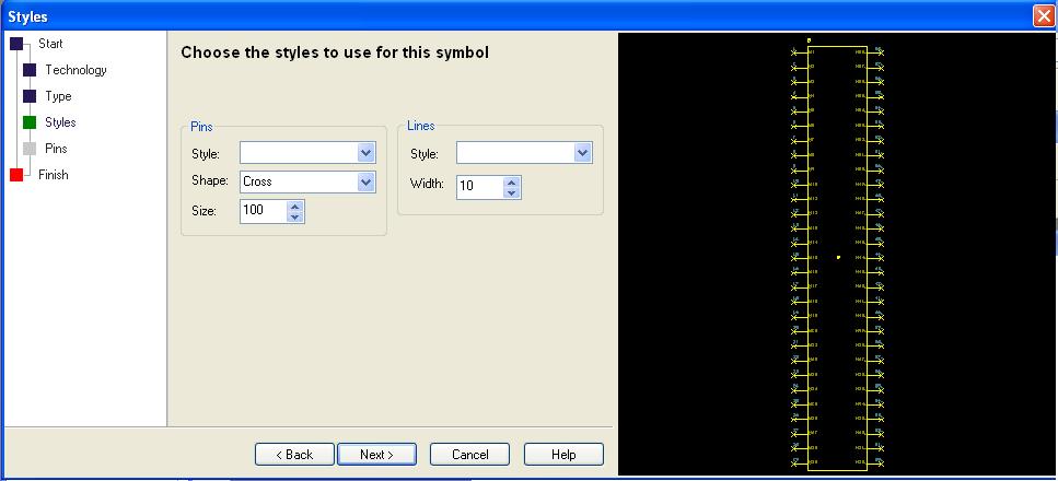
- In the next window, you can choose how you want the pins to be represented, the size of these and the length of the lines going to the pins. Leave these with the default values.
- Click 'Next'
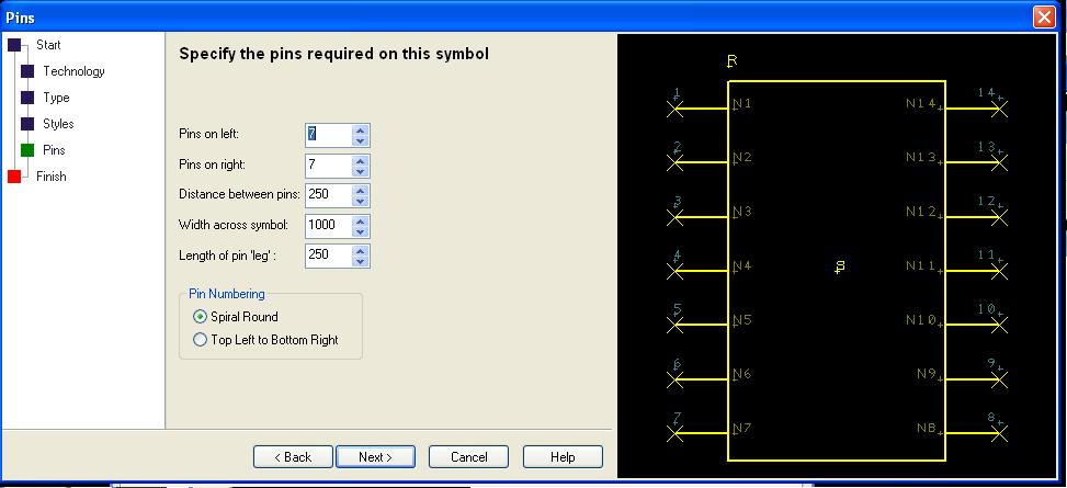
The next window determines the number of pins on each side of the component and some dimensions.
- Enter 7 for both Pins on left and Pins on Right.
- The other dimensions are not as important for the schematic, leave these as the default. (They can be editted later if too big or too small).
- The last part on this page describes how the pins are numbered. Since the schematic on the datasheet spirals the numbers, select the 'Spiral Round' option.
- Click 'Next'
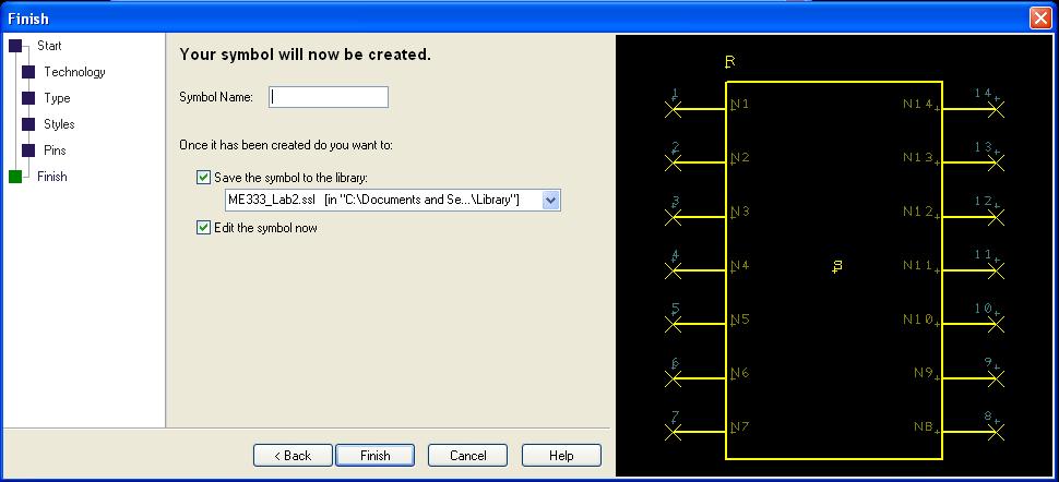
The last window is where you name the symbol and save it to a specific library.
- Name the component SN74HC04_Inverter and save it in the ME333_Lab2 Library that you downloaded above.
- Click Finish
You have now created a schematic symbol. If you checked the 'Edit the symbol now' box, you can see the schematic and edit if you want. We won't do any editting right now though.
Create a PCB Symbol
The next step is to create a pcb symbol for the component. This will be the footprint on your PCB. Look at the datasheet again and find the Plastic Dual-In Line Package footprint for the SN74HC04 (page 10). This tells us the dimensions we need for our footprint.
- Click on the Library Manager (blue book).
- Go to the PCB Symbols tab.
- Click on the Wizard again.
- Click Next on the start up window.
- On the Technology window, choose English with 'thou' as the unit and precision of 1. We choose this because it is the smallest unit on the datasheet for the English units.
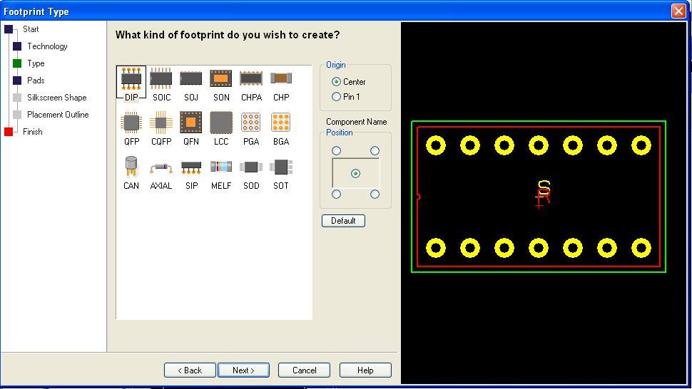
The next window is the footprint type.
- Select DIP type (the top left).
- For Origin - select center
- For Name - select center - this is where the name will be displayed on the PCB
- Click 'Next'
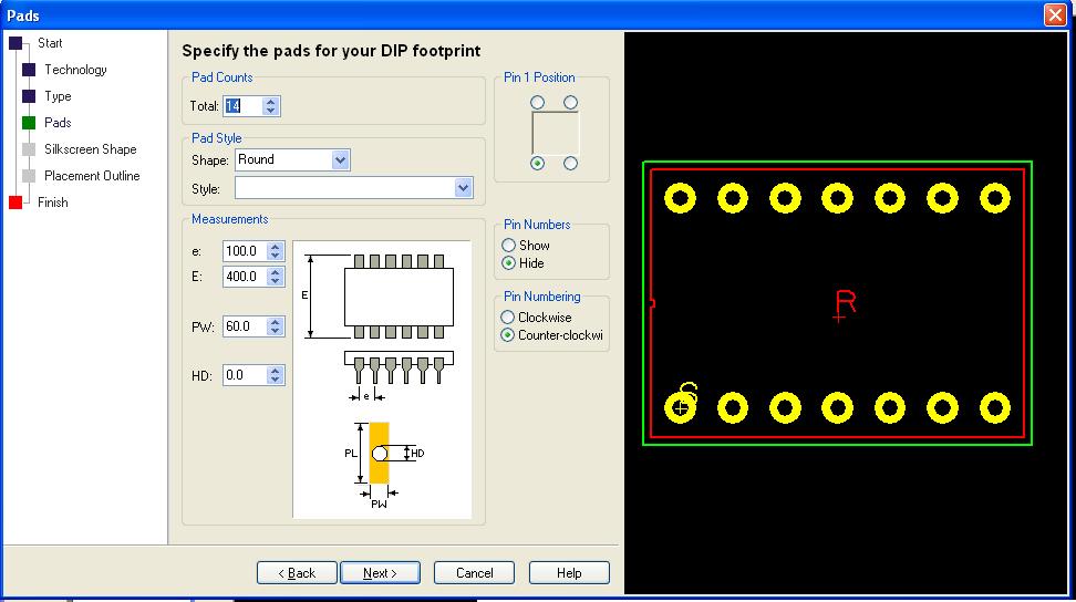
The next window describes the pads on the PCB. This window will be different for the different types of chips.
- Choose 14 pads
- For the Pad Style, choose 'Round' and leave Style blank.
The units are in thousands of inches
- e = 100 for 0.1 in pitch (as shown on the datasheet).
- E = 400. We can put this value between 325 and 430 as shown on the datasheet, but we also know that the chip can plug into a breadboard (spacings of 0.1 in), so 400 thou is a good number.
- PW = 60 and HD = 30. HD refers to the hole diameter for the pin. The pin diameter is around 20 thou as shown on the datasheet, so 30 thou is a good number with extra space. PW is the pad width (extra copper) surrounding the hole. Extra 30 thou is generally a good pad width.
- Choose Pin 1 Position to be the lower left corner (same as in the footprint on the datasheet)
- We don't want the pin numbers to be displayed on the PCB so select Hide for the Pin Numbers
- Pin number is counter clockwise.
- Click Next
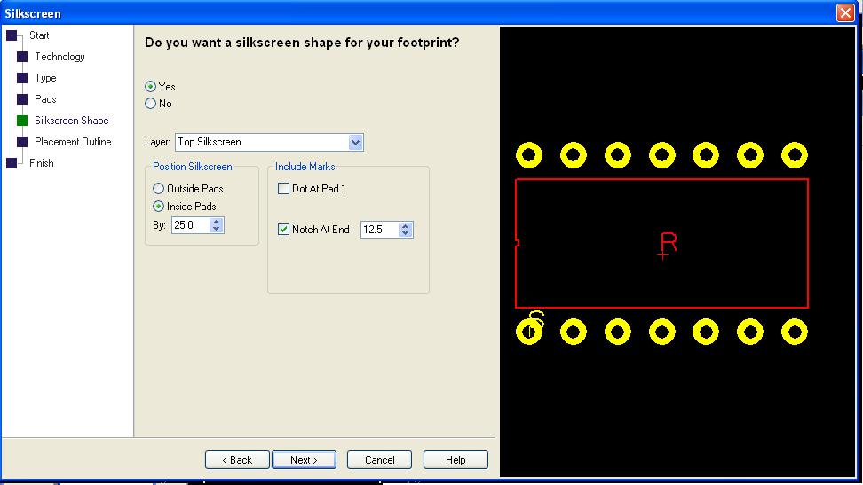
The next window describes the silk screen (the writing on top of the PCB).
- Click Yes
- Layer - Top Silkscreen
- Inside pads by 25 (sometimes you may want the silk screen to be outside the pads, but it is really your choice)
- Include Marks - Notch at end (12.5) --> this helps you figure out the orientation of the component
- Click Next
The next window asks if you want a placement shape (rectangle) around the entire component. We are not going to include this.
- Click No
- Click Next
- On the final window, name it SN74HC04_Inverter (same name as the schematic) and save it in the ME333 Library.
- Click Finish
You have now created a PCB footprint.
Create a Component
We created a schematic symbol and a pcb symbol above. Now we are going to create a component to link the two symbols.
- Click on the Library Manager and go to the Component tab.
- Click on the Wizard button
- Click Next on the opening window
The first window allows you to select what type of component you are making. You can make a Normal Component (both Schematic and PCB), only a Schematic component or only a PCB component.
- Select Normal Component
- Click Next
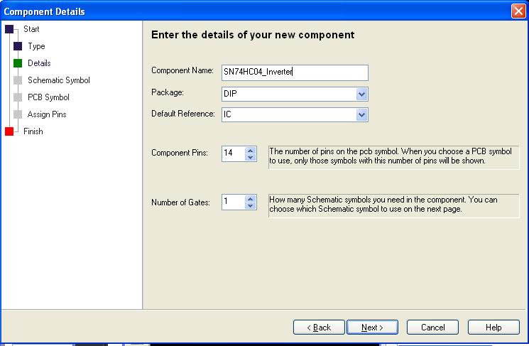
This windows contains the details for the component.
- Name = SN74HC04_Inverter (same as the symbols)
- Package - type DIP (this really doesn't matter)
- Default Reference - choose IC for integrated circuit
- Component pins - 14
- Number of Gates - 1 - this is the number of times your schematic symbol is needed for the component
- Click Next
In the next window you select the schematic symbol that you want to use
- Select SN74HC04_Inverter from the ME333 Library
- Click Next
In the PCB window, you select the pcb symbol that you want to use
- Select SN74HC04_Inverter from the ME333 Library
- Click Next
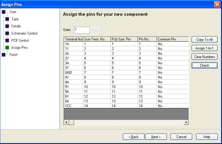
The next window assigns the pins from the schematic to the pcb. Since we choose our pins in the schematic and pcb to have the same order:
- Select Assign 1-to-1 button to assign Pin 1 Schematic to Pin 1 PCB ... etc
We can also choose to add names to each pin.
- Assign the pins names (1A,1Y,GND..etc) to each of the pins as shown on the datasheet.
- Click Next
On the final window:
- Click Save the component to the library --> Put it in the ME333 library
If you want to edit the component now (check the next box)
- Click finish
You have now created a component and can use it with schematics and pcbs.
Practice Making a PCB
After reviewing this tutorial, you are ready to Practice Making a PCB.
